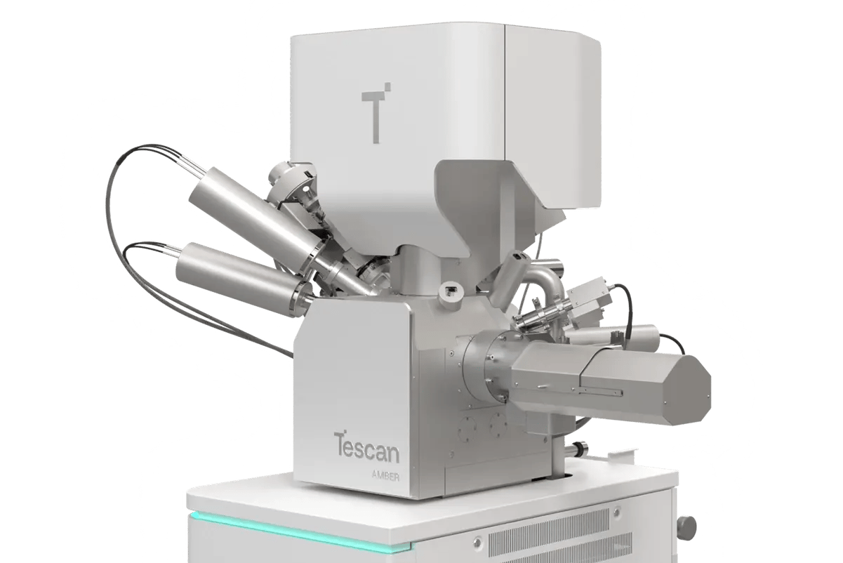
WEBINAR | From Infrastructure to Impact: EM & Micro-CT in Materials Core Facilities

From Design to device: Prototyping of Gallium-Doped Silicon Nanowires

From focused ion implantation to electrical testing—entirely within one FIB-SEM Instrument.

hero
hero
Unlocked content

Bringing Device Prototyping Down to the Nanoscale

Turning a single silicon nanowire into a functional electronic element takes more than material synthesis. It requires precise control over doping, geometry, placement, and electrical interfacing.

In conventional setups, device prototyping demands a broad range of instruments and technical expertise, making the workflow more complex and time-consuming. Performing the entire process within a single FIB-SEM significantly streamlines iteration, reducing both time and risk of contamination.

This case study shows how a Tescan FIB-SEM system streamlines prototyping. Gallium ion implantation, nanowire manipulation, EBL-based contact patterning, and electrical testing are all performed in situ—within the same chamber and under unified control. Anisotropic wet etching, done externally, fits into the workflow without disrupting alignment or sample integrity.

Why a Single-Platform Approach Makes Sense

01
Root of the Problem

Building testable nanowire devices without breaking the workflow

Silicon nanowires offer excellent material properties for sensing and prototyping, but leveraging those properties for functional device evaluation requires precise, integrated handling. Traditional workflows rely on multiple instruments for implantation, etching, contact fabrication, and electrical measurement.

Each handoff risks structural damage, contamination, or misalignment, compromising both the yield and the repeatability of measurements. A better strategy is to consolidate these steps into a single, automated environment. 

02
Materials and Methods

Ion Implantation, Nanowire Manipulation, and Electrical Contact Fabrication — All Inside One System

The process began with focused gallium ion implantation into selected regions of a Si substrate using a Tescan FIB-SEM (30 keV, 200 pA). The implanted zones served as both doping source and etch mask.

After implantation, samples were etched in 30% KOH at 50 °C. This revealed freestanding, doped nanowires with widths in the hundreds of nanometers and a typical height of ~55 nm.

Contact pads were patterned via electron beam lithography (EBL) inside the FIB-SEM chamber. A resist layer was exposed to define the pad geometry, followed by Ti/Au deposition and lift-off, leaving the metal contacts in place on the SiO₂-coated substrate.

This in situ approach enabled seamless transition to nanowire integration. Nanowires were then lifted with the in-column manipulator, positioned onto the contact platform, and welded in place using focused ion beam-induced deposition (FIBID).

Final cuts released the nanowires from the manipulator, and I–V measurements were taken immediately. AFM was used to confirm nanowire dimensions and placement accuracy.

03
Results and Discussion

Functional nanowires fabricated and tested without leaving the system

Every step — from ion implantation, EBL-based contact fabrication, pickup, placement, to electrical testing — was performed inside the Tescan FIB-SEM.

Anisotropic etching, done externally in a KOH wet bath, was integrated into the workflow without disrupting alignment or geometry. The nanowires retained uniform structure throughout, and placement precision enabled direct contact formation without distortion.

Electrical tests showed stable, linear I–V behavior, with conductivity increasing as a function of gallium dose. No Schottky barriers or current instability were detected, confirming both the effectiveness of doping and the cleanliness of the contact interfaces.

This integrated workflow demonstrates how silicon nanowires can be transformed into working devices without leaving the fabrication environment, supporting rapid development of nanoscale sensors, interconnects, and logic elements from a single nanostructure. 

GET IN Touch

Contact us

Get the most out of Tescan

This is more than information; it's an advantage. We've compiled our technical whitepapers, detailed product flyers, and on-demand webinars to provide you with the knowledge that makes a real difference. Sign up now to access the insights you need to make an impact.

Tescan Instruments & Technology

Used in This Workflow

Tescan AMBER with Nanoprototyping Toolbox™

Tescan AMBER is a multi-functional FIB-SEM system designed for advanced nano-prototyping and in-situ device preparation.

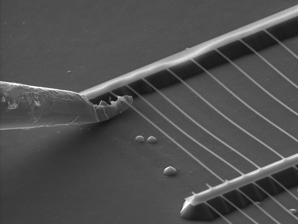
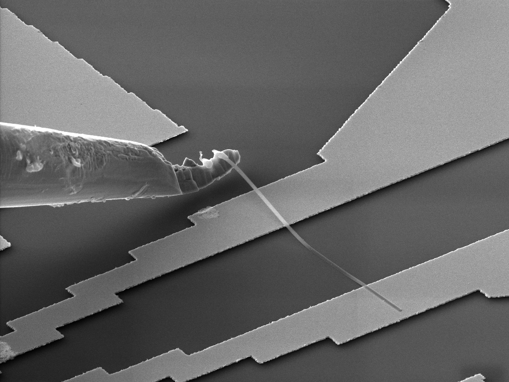
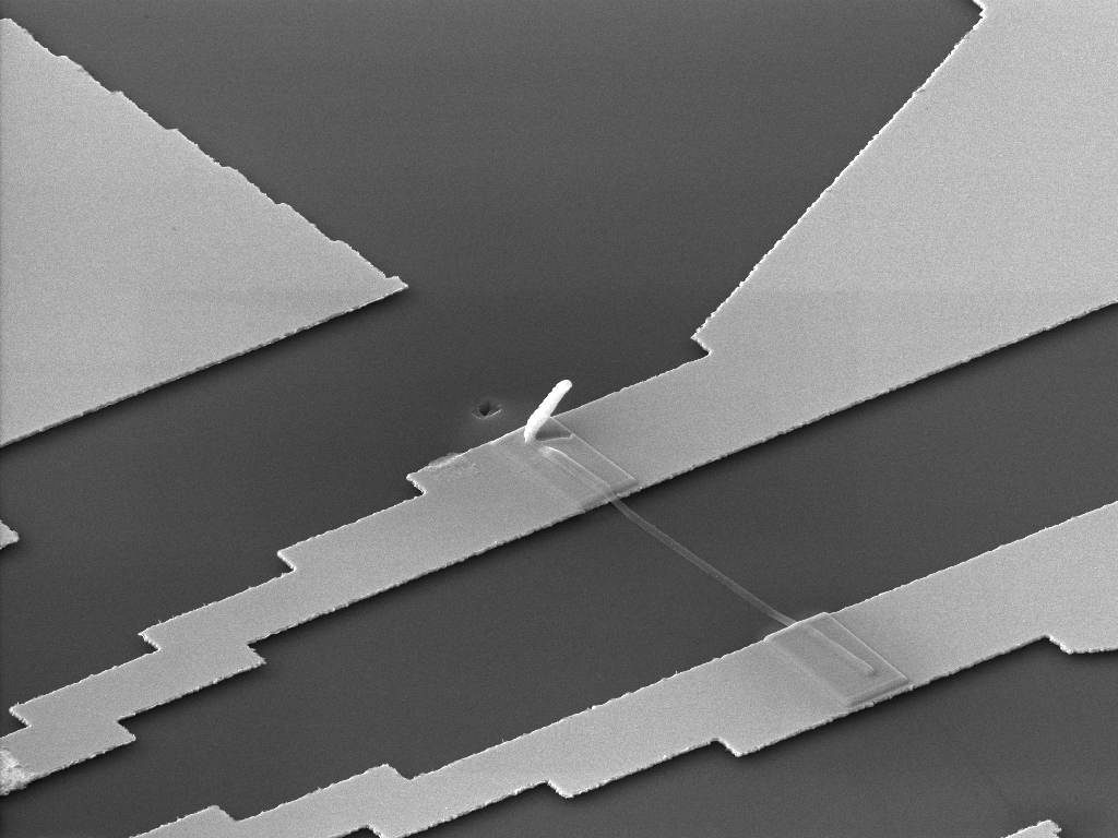
It combines high-precision gallium ion beam milling, high-resolution SEM imaging, and integrated nanomanipulation — all within a fully controlled environment.

This enables complete workflows for ion implantation, nanowire lift-out, and electrical contact integration without transferring the sample between systems.

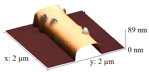
  • Gallium FIB: enables precise ion implantation and FIB-induced deposition (FIBID)
  • In-chamber nanomanipulator: supports accurate lift-out, placement, and alignment of 1D nanostructures
  • Real-time SEM imaging: enables precise visual feedback and supports focused electron beam-induced deposition (FEBID)
  • Direct gas injection: enables precise material deposition using electron or ion beams to modify or fabricate the sample
  • Seamless integration: ideal for closed-loop prototyping and device-level testing at the nanoscale
AMBER 2

Tescan SOLARIS with Nanoprototyping Toolbox™

Tescan SOLARIS is a high-resolution FIB-SEM platform optimized for ultra-precise nanofabrication and in-situ lithography.

Featuring advanced electron optics and the Nanoprototyping toolbox, it enables high-fidelity patterning — including EBL-based contact fabrication — directly within the vacuum chamber.

This supports seamless integration of electrical contacts into functional nanoscale devices without breaking workflow continuity.

  • Nanoprototyping Toolbox™: enables direct-write lithography and complex structure definition
  • EBL-enabled system: fabricate contact pads without removing the sample from the FIB-SEM
  • Direct gas injection: supports localized material deposition for contact formation or structural modification
  • Optimized platform for in situ lithography: advanced stability for accurate resist exposure and pattern transfer
SOLARIS (2)

GET IN Touch

Contact us

map

Where can you find us:

Tescan Brno
Libušina třída 21
623 00 Brno
Czech Republic

info@Tescan.com 

130405923 us US 37.09024 -95.712891 25.3575 29.349345 20.67957527 42.082797 39.91384763 -33.693421 13.93320106 3.039986586 31.997988 38.050985 47.579533 48.1485965 58.375799 54.663142 19.195447 56.975106 50.493053 45.868592 10.79556993 44.35660598 43.2371604 55.536415 14.557577179752773 32.100937 -6.116829 -6.212299277967318 23.7104 -33.471062 31.998740087 -23.69149395 43.462349 51.529848 49.1893523 49.197486 25.072375 31.075811 1.299027 40.676979 52.30150662 51.013813 35.684121 37.479653 52.246622 40.581349 39.911632 -26.1811371 41.818215 33.429928

No distributors found.