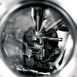
WEBINAR | Up to 40% Faster Automated TEM Lamella Preparation with new Ga⁺ FIB Column

High-Temperature Ion Implantation for NV Center Formation in Diamond

Generating shallow, high-density NV ensembles using Tescan QuiiN with high precision. 

hero
hero
Unlocked content

High-Temperature Ion Implantation for Precise NV Center Engineering in Diamond

Creating nitrogen-vacancy (NV) centers is key to building diamond-based quantum sensors, but doing so without damaging the crystal has long been a challenge. Conventional ion implantation often forces a tradeoff: use high fluence to get more NVs, and risk damaging the lattice, especially near the surface, where graphitization can suppress photoluminescence.

This application example shows how the Tescan QuiiN system, with its focused ion beam and heated stage, enables precise nitrogen implantation at 800 °C. The result is a high-density layer of NV centers, confined to a depth of 15 nm below the surface, with no structural damage and excellent optical quality.

Why Use High-Temperature Implantation

for NV Center Creation?

01
Root of the Problem

Balancing yield and damage in near-surface NV engineering

For NV centers to work as quantum sensors or spin platforms, they need to be both bright and precisely placed, typically within 20 nm of the diamond surface. But hitting this sweet spot is challenging.

At room temperature, higher ion fluence can cause damage to the materials lattice around the desired NV, causing amorphization and leading to a loss in performance. The result is reduced brightness or even elimination of the photoluminescence effect altogether.

The solution lies in managing the tradeoff: maintaining enough defect density while avoiding structural breakdown

02
Materials and Methods

High-temperature nitrogen implantation using the QuiiN system

Nitrogen ions (N₂⁺) were implanted at 30 keV into electronic-grade CVD diamond using Tescan QuiiN, equipped with a focused iVeloce ion column and heated stage.

Implantation was carried out at both room temperature and 800 °C for comparison. Ar⁺ ions were used to mark regions with ring patterns for post-alignment. After implantation, all samples were annealed at 800 °C for one hour.

Implant depth was ~10–15 nm. NV patterning was performed with high spatial control. Characterization was done via confocal photoluminescence (PL), Raman spectroscopy, and DiamondView imaging at 80 K using 532 nm laser excitation.

03
Results and Discussion

Bright, Shallow NV Centers Without Crystal Damage

Room temperature implantation at high dose led to graphitization and a weaker PL signal. In contrast, the high-temperature process produced:

  • 3–4× stronger NV photoluminescence
  • No signs of amorphization or lattice damage
  • Dense NV populations near the surface
  • Consistent results across multiple patterned sites

The elevated temperature enabled dynamic lattice recovery, preventing damage accumulation even at fluences above 10¹⁴ ions/cm².

These results highlight the power of the Tescan QuiiN system for precision quantum defect engineering. In addition to NVs, the same workflow could support formation of SiV, GeV, or co-doped NV–He⁺ structures. With high-precision and full pattern control in the FIB, this approach is well suited for quantum sensing, spin physics, and photonics research.

GET IN Touch

Contact us

Get the most out of Tescan

This is more than information; it's an advantage. We've compiled our technical whitepapers, detailed product flyers, and on-demand webinars to provide you with the knowledge that makes a real difference. Sign up now to access the insights you need to make an impact.

Tescan Instruments & Technology

Used in This Workflow

Tescan QuiiN

A precision implantation system designed for quantum materials and defect engineering.

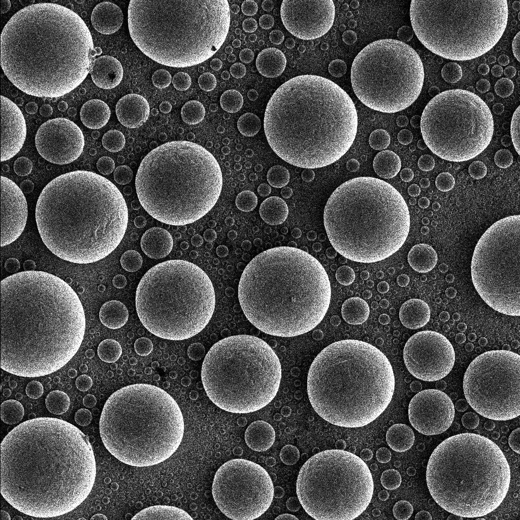
  • Mass-filtered Veloce LMAIS and iVeloce plasma ion column for O, N, Si, He, and a myriad of custom species

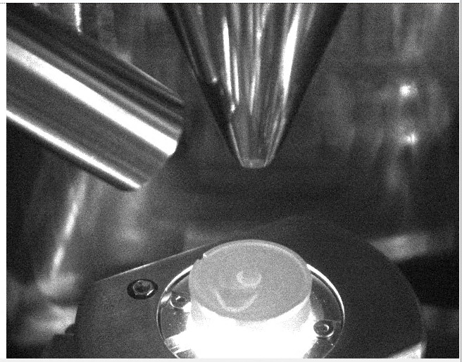
  • Heating stage supporting in-situ implantation up to 900°C

  • Control depth by changing the accelerating voltage of the primary ions

  • Compatible with cryogenic workflows, annealing, and post-exposure imaging

GET IN Touch

Contact us

map

Where can you find us:

Tescan Brno
Libušina třída 21
623 00 Brno
Czech Republic

info@Tescan.com