![[Left] Result of the height calibration test. [Right] Result of the sigma calibration test. Both datasets are used to calibrate the growth rate parameters for the final 3D deposition process.](https://tescan.com/hubfs/Nov%C3%BD%20projekt%20(12).webp?hsLang=en)
.webp?hsLang=en)
.webp?hsLang=en)
.webp?hsLang=en)
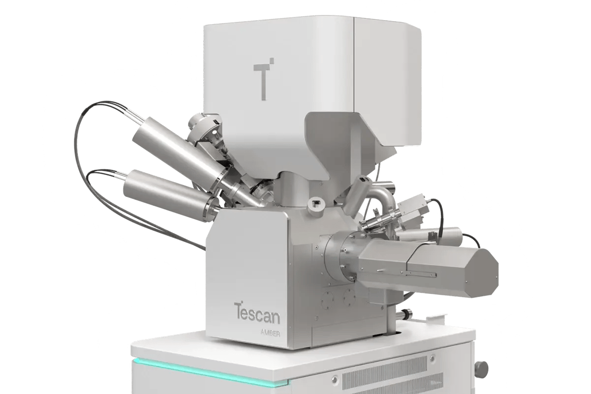
Tescan AMBER™ with FIB-SEM Expert PI™ API
Tescan AMBER™ combines high-precision gallium FIB milling with ultra-high-resolution SEM imaging in a versatile dual-beam platform.
As part of the nanoprototyping toolbox™, AMBER™ can be paired with the Tescan FIB-SEM Expert PI™ API (Application Programming Interface) to enable fully automated 3D nanofabrication workflows such as proximity-corrected Focused Electron Beam-Induced Deposition (FEBID).
You can control beam, stage, and gas on/off parameters directly from scripted recipes — ensuring reproducible, high-fidelity nanostructures without manual intervention.
- Gallium FIB: Sub‑micrometer milling and site‑specific cross‑sectioning
- Integrated SEM: Nanoscale imaging and process monitoring
- FIB-SEM Expert PI™ API: Direct scripting for automated beam and gas control
- Stream File protocol support: Execute complex, layer‑by‑layer deposition routines
- Gas injection compatibility: Deposit functional or structural materials in situ