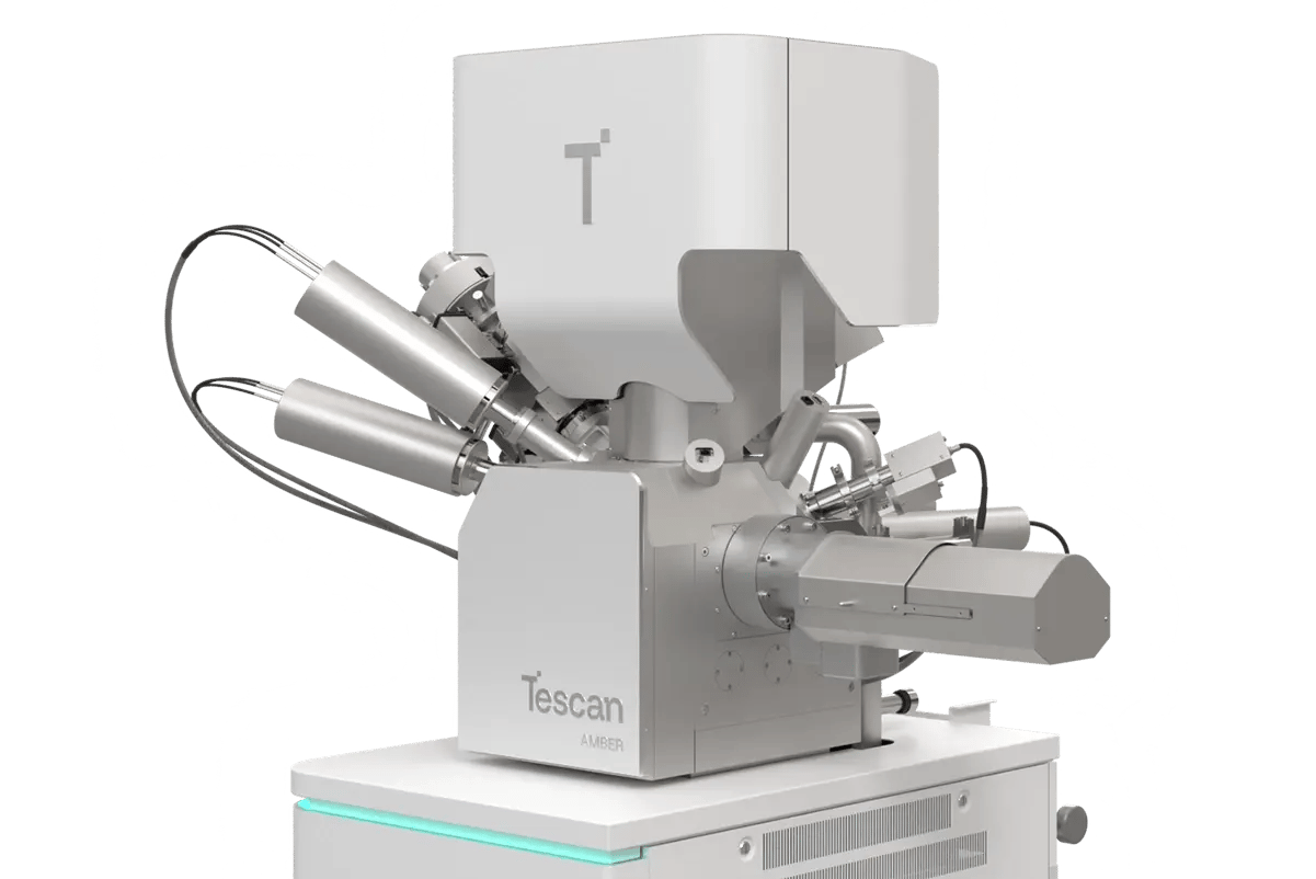
Tescan AMBER™
Combining high‑precision milling, ultra‑high‑resolution imaging, and advanced automation for materials research and TEM sample preparation, Tescan AMBER™ enables researchers to perform site‑specific cross‑sectioning, 3D tomography, and correlative imaging workflows with exceptional accuracy and repeatability.
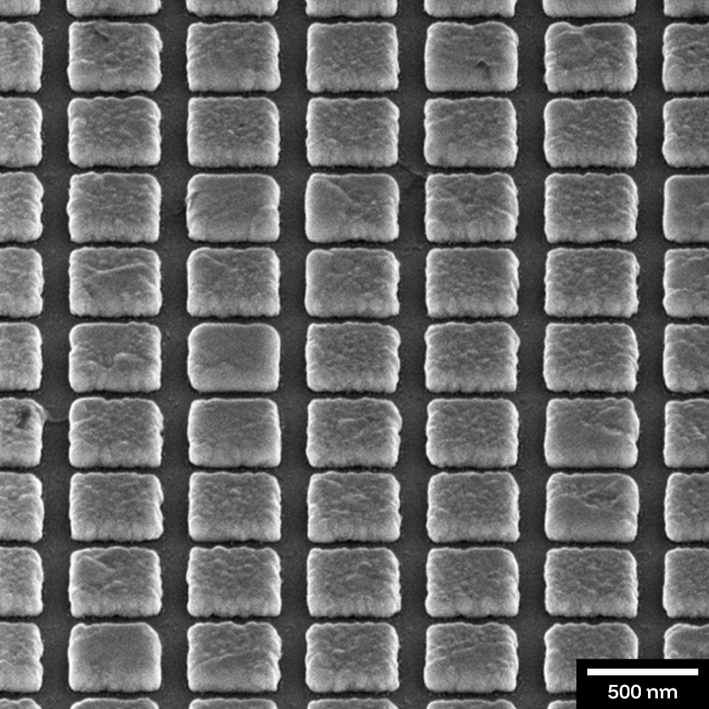
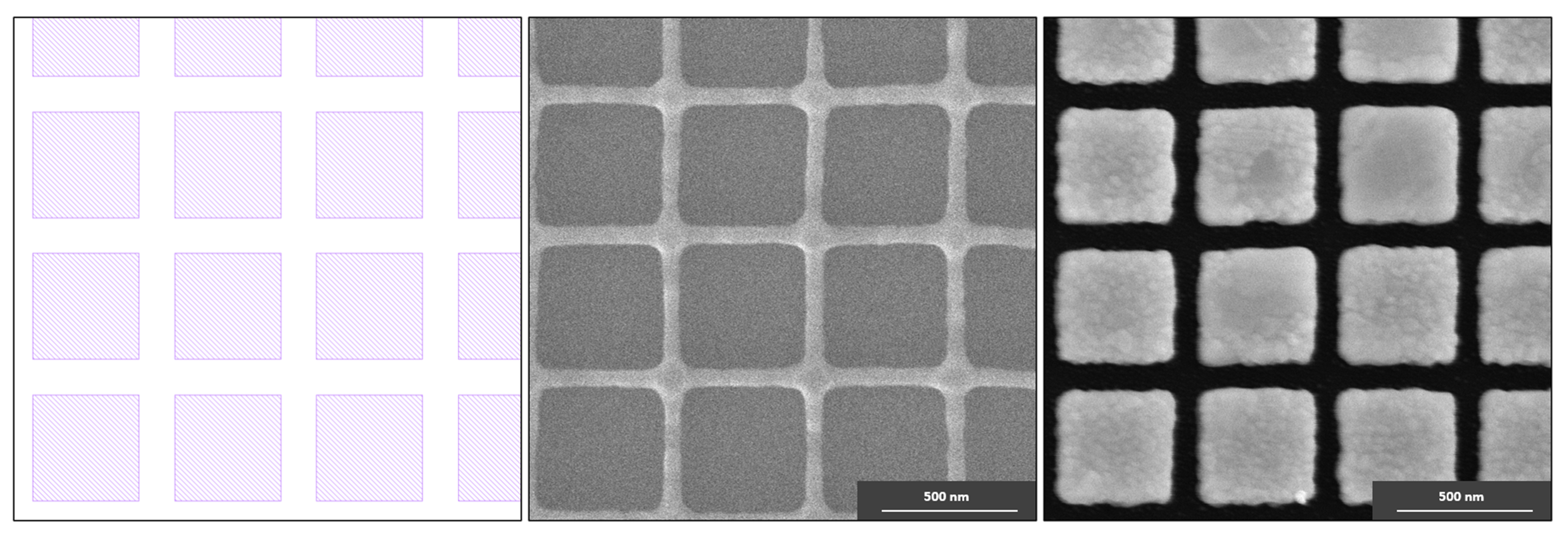
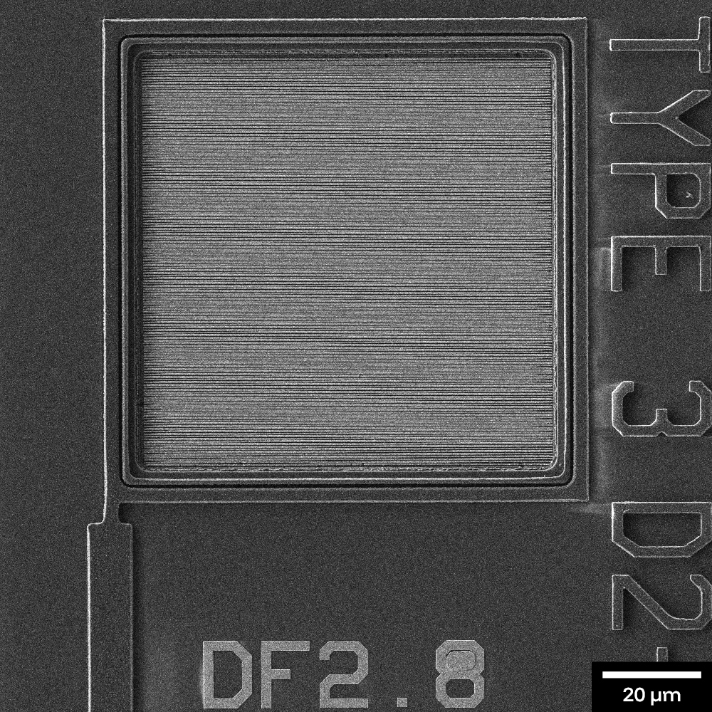
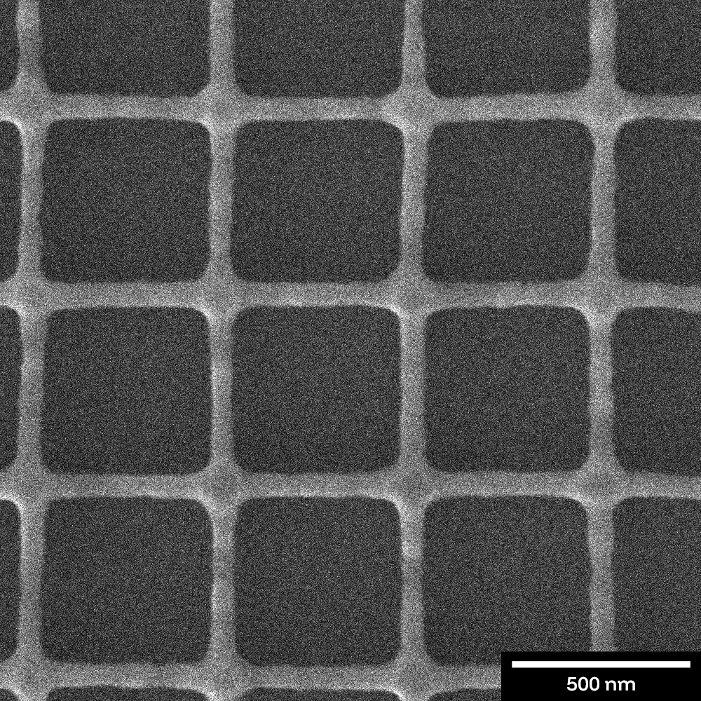
- Gallium FIB: High‑precision nanofabrication,cross‑sectioning and TEM prep
- Ultra‑high‑resolution SEM: Detailed imaging, structural analysis and electron beam lithography
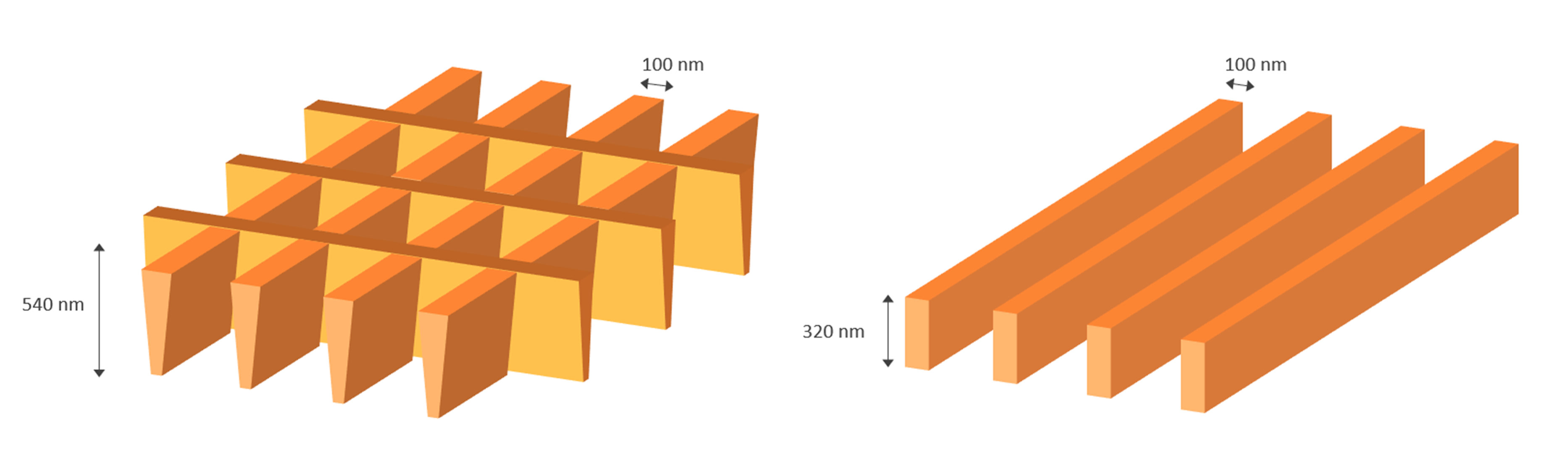
- Nanoprototyping Toolbox™: Extends AMBER™’s capabilities into advanced nanostructuring and prototyping workflows
- Advanced automation: Streamlined repetitive tasks and enable complex workflows or prototyping
- Gas Injection System (GIS): Enables in-situ deposition, etching, and enhanced milling strategies
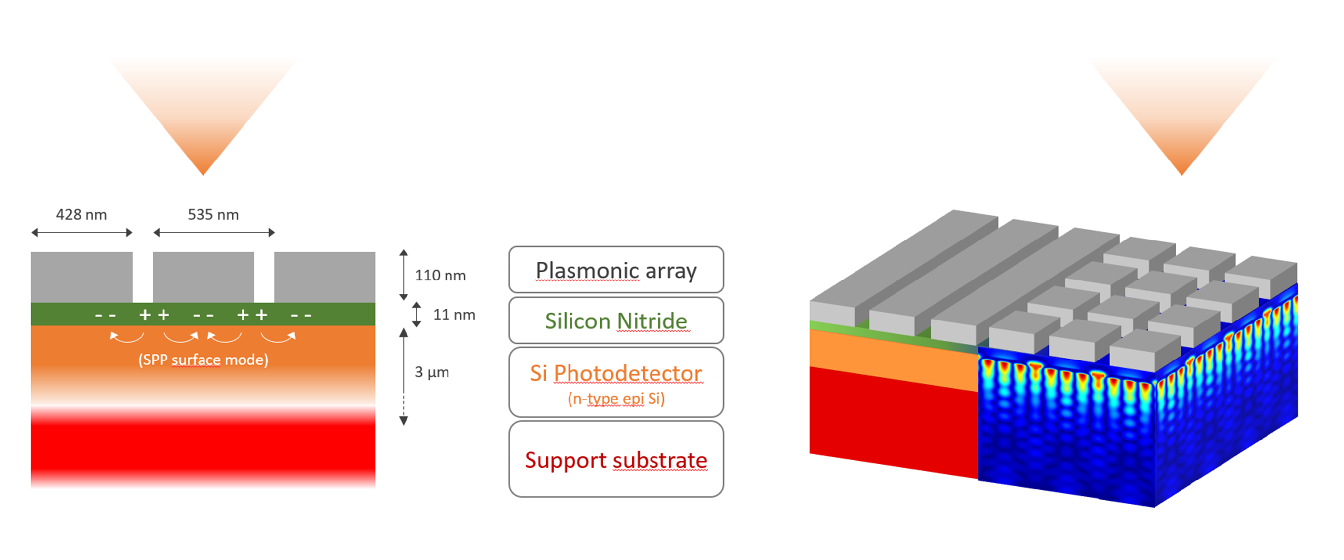
- Application focus: Nanophotonics, plasmonics, surface modification, and novel material research including 2D materials and magnonics.