WEBINAR | Up to 40% Faster Automated TEM Lamella Preparation with new Ga⁺ FIB Column

Engineering the Cell Surface Environment with Nanoscale Protein Patterns

TESCAN’s EBL workflow enables precise ligand placement to control receptor clustering and cellular signaling.

hero
hero
Unlocked content

Rewriting Cell Signaling, One Nanopattern at a Time

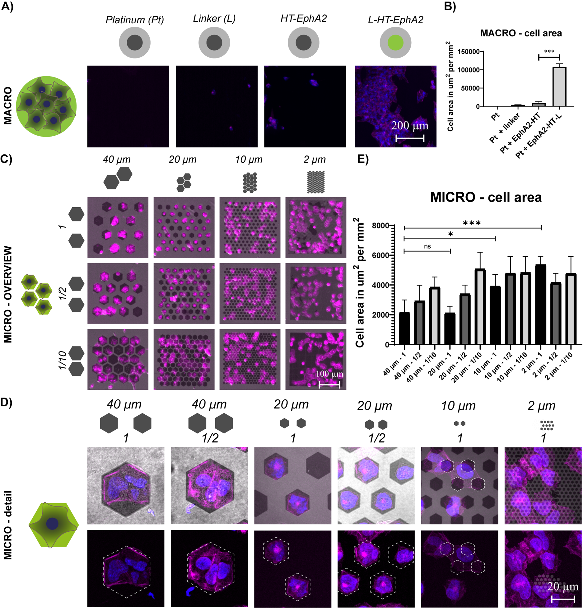
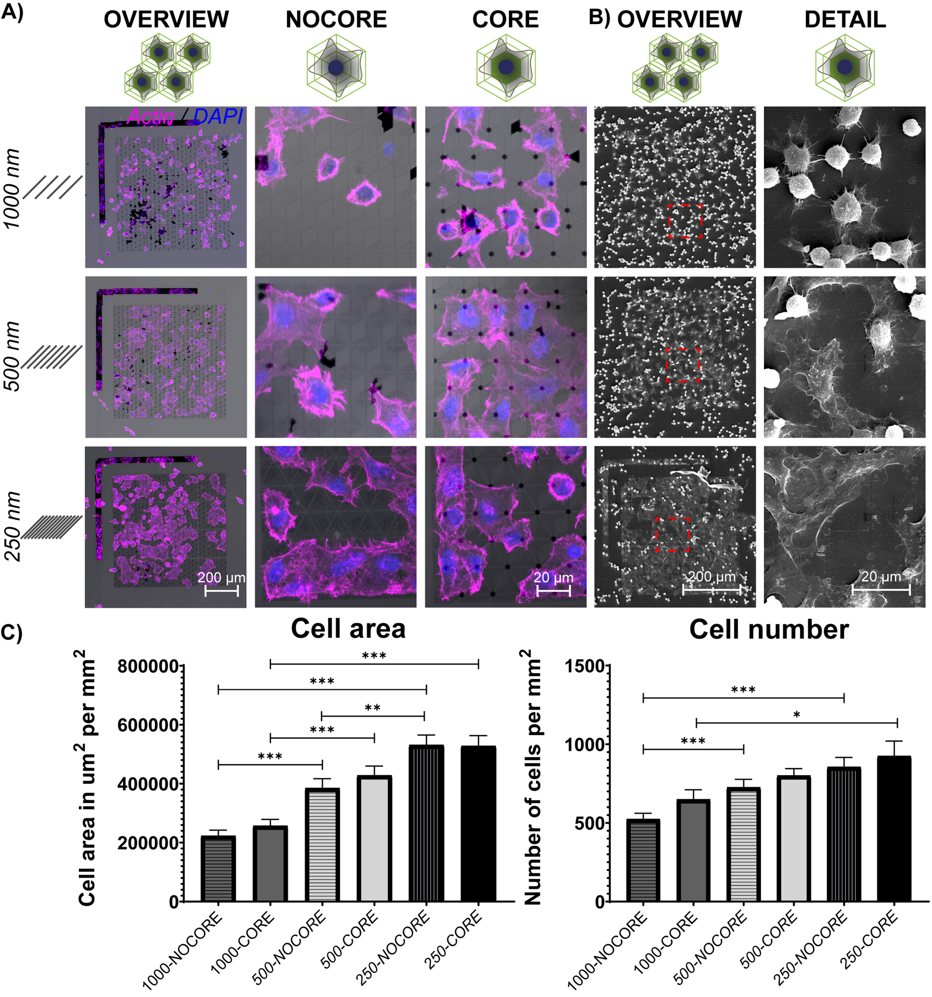
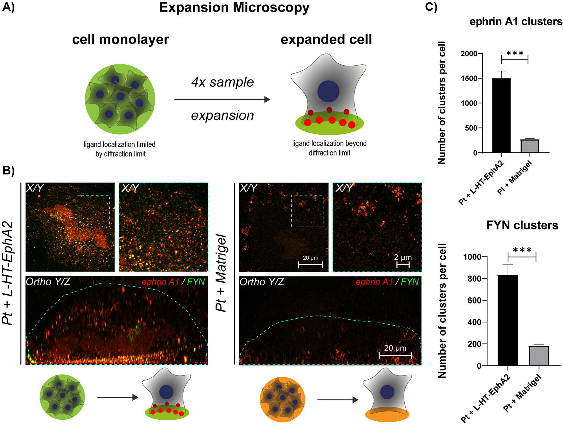
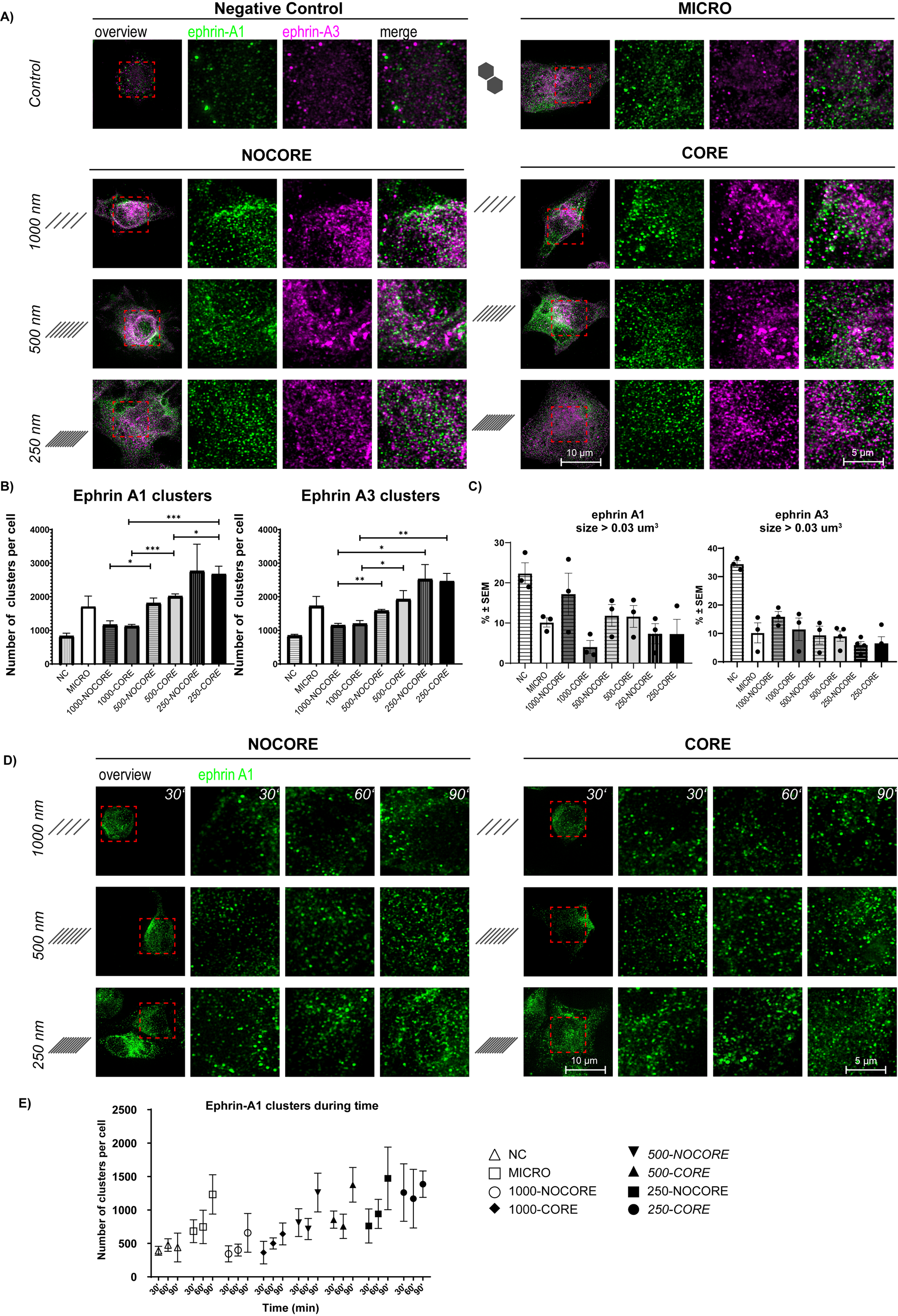
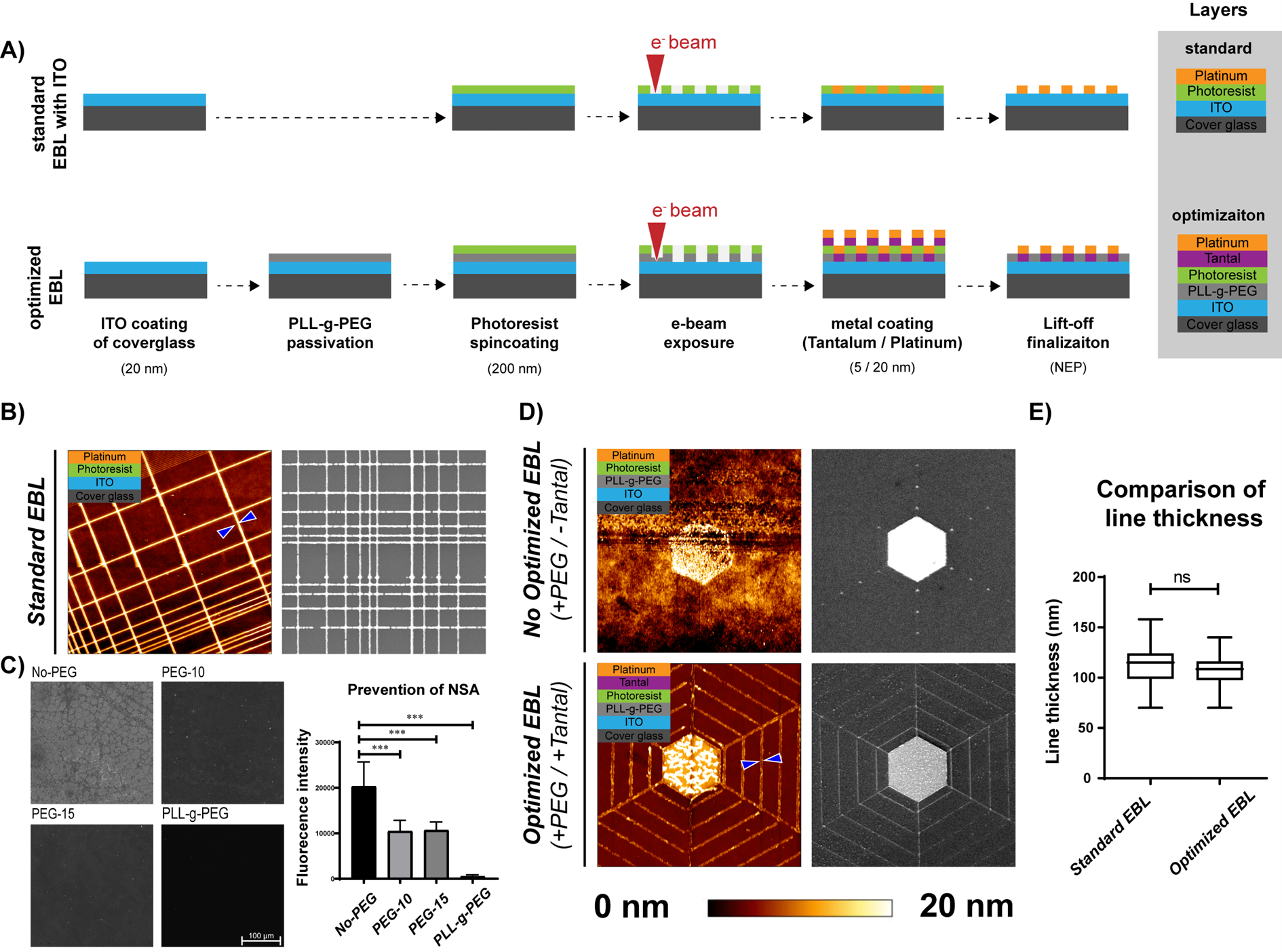
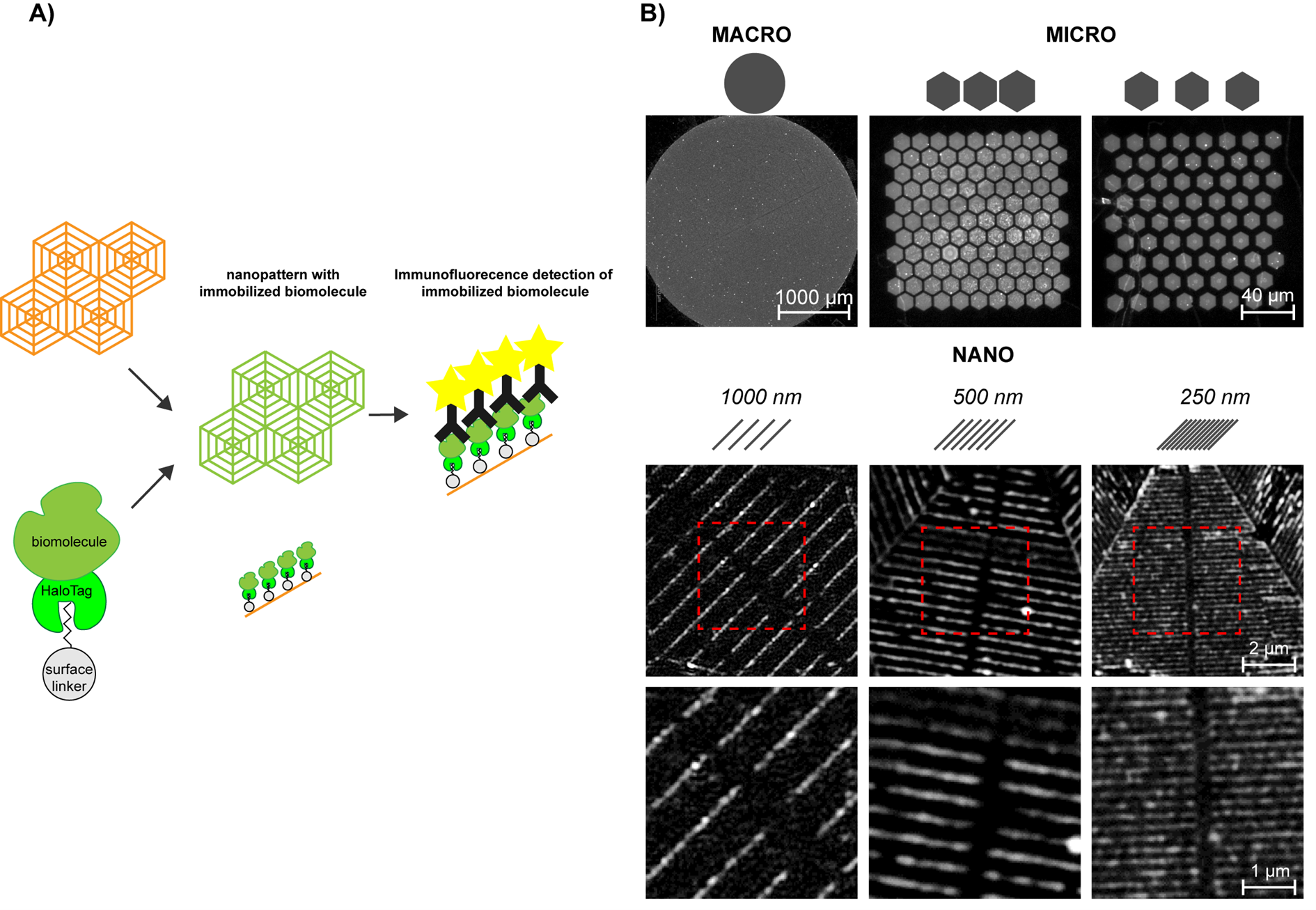
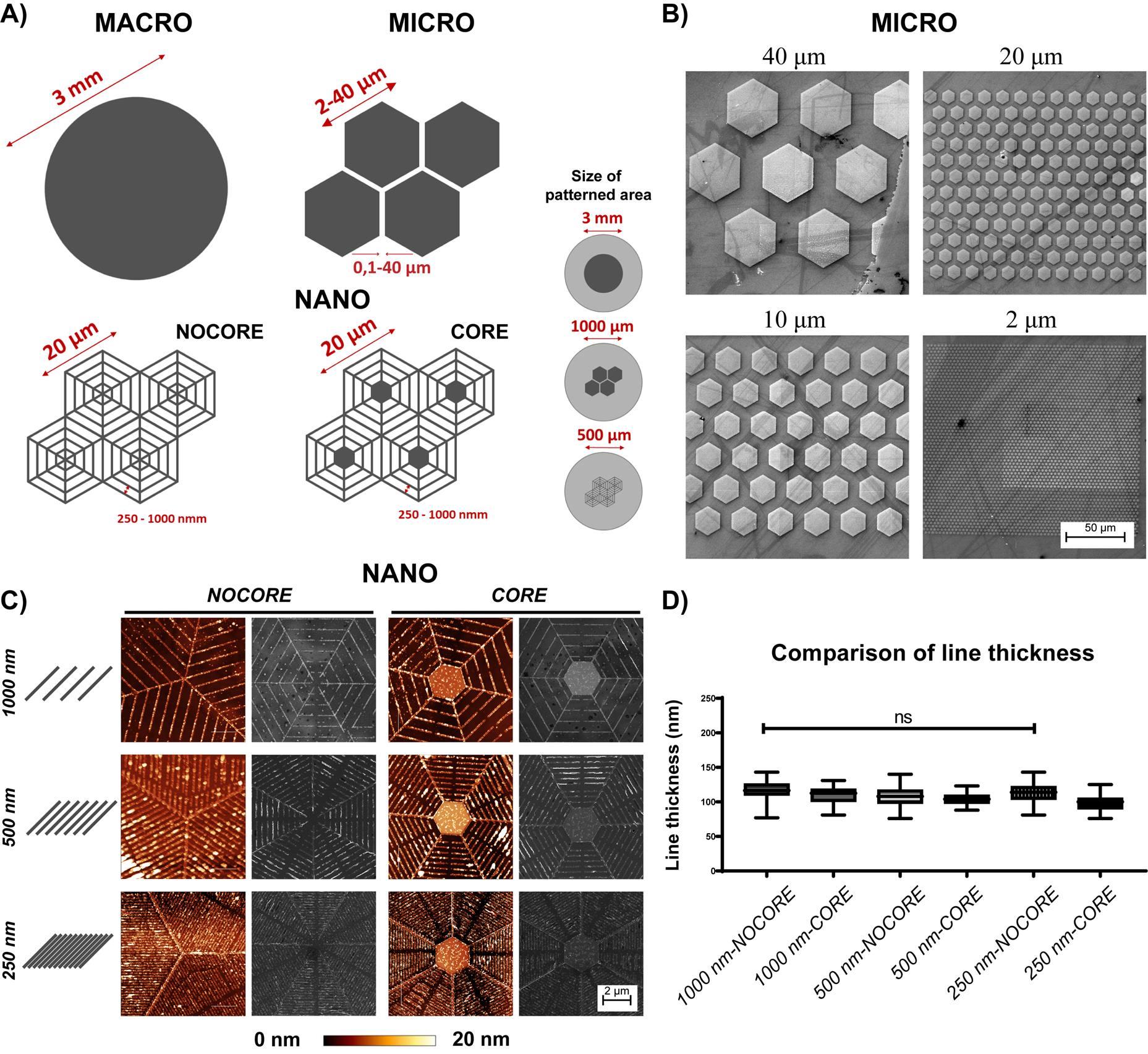
Cells respond not only to which ligands are present, but where they are, how many there are, and how they’re arranged. Spatial distribution at the cell–surface interface plays a key role in triggering adhesion, receptor clustering, and signal transduction. Yet building biofunctional nanostructures with this level of precision often comes at the cost of resolution or compatibility with living systems.

This example highlights a robust SEM-based nanopatterning workflow using TESCAN technology to precisely present membrane proteins like EphA2. With patterns spaced down to 250 nm, researchers can systematically explore how nanoscale architecture shapes stem cell behavior and intracellular signaling.

Why Use Electron Beam Lithography

for Cell–Surface Engineering?

01
Root of the Problem

Understanding receptor behavior takes more than just surface chemistry

Standard substrates typically offer static or randomly distributed ligands, but receptor systems like EphA2 are highly sensitive to spatial arrangement. They don’t just react to presence, but also respond to nanoscale clustering, density, and order.

To investigate how spatial architecture drives signal activation, researchers need a way to fabricate ligand patterns with nanoscale precision, on surfaces that are biologically and optically compatible. That’s where electron beam lithography makes the difference.

02
Materials and Methods

Creating protein-functionalized nanogrids for cell interaction studies

Glass coverslips were cleaned, PEGylated, and coated with 20 nm of indium tin oxide to prevent charging during patterning. Hexagonal platinum nanogrids were written using TESCAN MIRA3 and MIRA4 SEMs equipped with the Essence™ EBL Kit. Three spacings were tested: 1000, 500, and 250 nm.

Exposure doses were optimized for each geometry:

  • 92 μC/cm² for the widest pitch

  • 86 μC/cm² for the highest-density patterns

To ensure stability and bioactivity, grids were sputter-coated with 5 nm Ta and 20 nm Pt. Ligand presentation was achieved by conjugating HaloTag-EphA2 proteins to the platinum via thiol chemistry. Human pluripotent stem cells were then seeded onto the patterns and analyzed using SIM and expansion microscopy to track receptor behavior, adhesion, and FYN kinase signaling.

03
Results and Discussion

Cells read nanoscale architecture – and respond accordingly

All patterns successfully immobilized HaloTag-labeled EphA2 proteins, but cellular behavior varied with grid density:

  • At 1000 nm spacing, cells adhered weakly and showed low receptor activation.
  • At 500 and 250 nm, cells spread more broadly and formed robust focal adhesions.

Higher-density patterns also promoted Ephrin clustering and strong colocalization with FYN kinase, indicating functional signal transduction.

These results show that nanoscale patterning doesn’t just support cell attachment. What’s more, It shapes how cells interpret and respond to their environment. TESCAN’s EBL workflow proved consistent, scalable, and compatible with both biological assays and high-resolution imaging, offering a powerful tool for engineering the cell–material interface.

GET IN Touch

Contact us

Get the most out of Tescan

This is more than information; it's an advantage. We've compiled our technical whitepapers, detailed product flyers, and on-demand webinars to provide you with the knowledge that makes a real difference. Sign up now to access the insights you need to make an impact.

GET IN Touch

Contact us

map

Where can you find us:

Tescan Brno
Libušina třída 21
623 00 Brno
Czech Republic

info@Tescan.com