WEBINAR | Up to 40% Faster Automated TEM Lamella Preparation with new Ga⁺ FIB Column

Rapid Development of Functional Devices at Nanoscale  


Seamless integration of milling, deposition, ion implantation and electron beam lithography makes it possible to fabricate and refine device features directly in the microscope. Streamline research and accelerate development with faster, more efficient nanoprototyping.

Nanoprototyping
Nanoprototyping

Contents

3D Nanoprinting for the next generation of devices

Combine open-source f3ast software with Tescan’s FIB-SEM Expert PI API to enable proximity-corrected, automated 3D nanoprinting workflows inside FIB-SEM systems. This integration delivers reproducible fabrication of complex nanostructures with precision and speed, accelerating the path from concept to device.

  • Open-source workflow: f3ast software generates optimized recipes from 3D models

  • API-based automation: Direct execution through the Tescan’s FIB-SEM Expert PI interface

  • Growth and sigma calibration: Guarantees accurate height and geometry control
  • Validated outcomes: Successful fabrication of spiral balls, helices, and other 3D nanoscale geometries
spiral ball 1 (1)
Avalanche detector – single photon detector for plasmonics research

Integrate high-density plasmonic nanoarrays directly onto silicon photodetectors to boost near-infrared photon absorption. This electron-beam lithography workflow delivers precise alignment, reproducible fabrication, and up to threefold efficiency enhancement without degrading device performance.

  • Nanoscale patterning: Silver nanostrips (1D) and nanosquares (2D) fabricated with sub-10 nm precision
  • Optimized resist & beam parameters: Ensures stable structures with lift-off compatibility
  • Plasmonic enhancement: Surface plasmon polaritons confine light, increasing NIR absorption
  • Validated performance: Demonstrated ~45% quantum efficiency improvement at 950 nm
fig 1-2
High-Temperature Ion Implantation for NV Center Formation in Diamond

Use Tescan QuiiN with a heating stage and focused ion beam to engineer shallow, high-density NV centers in diamond at 800 °C. This workflow enables colour center creation with precision and brightness while preventing crystal damage.

  • Focused ion beam precision: Control NV center placement with high accuracy
  • High-temperature implantation: In-situ lattice recovery prevents graphitization at high fluence
  • Bright shallow NVs: 3–4× stronger photoluminescence compared to room temperature processes
  • Stable spin properties: ODMR validation confirms narrow linewidths for quantum sensing
  • Versatile quantum defects: Supports NV as well as SiV, GeV, and co-doped structures
img5 (4)
Nanostructured surface for embryonal cell research

Leverage optimized electron beam lithography with biomolecule tethering to fabricate large-area nanopatterns that control cell behavior. This workflow enables precise nanoscale distribution of proteins, revealing how geometry influences adhesion, spreading, and signaling in human stem cells.

  • High-resolution nanopatterning: Sub-100 nm hexagonal arrays across 500 × 500 µm² areas

  • Biocompatible surfaces: ITO coatings for conductivity, Platinum structures for biocompability and PEG layers to block nonspecific binding

  • Scalable design: MACRO (mm), MICRO (µm), and NANO (nm) patterns for multi-scale cell studies

  • Functional outcomes: Pattern density modulates ephrin clustering and FYN colocalization, confirming nanoscale control of signaling
Figure 2-3
Prototyping of 1D systems Si Nanowires study

Leverage a fully integrated FIB-SEM workflow to fabricate, manipulate, and characterize gallium-doped silicon nanowires. This approach unifies implantation, electron beam lithography of conductive contacts, placement, and electrical testing within one system, accelerating sensor development and ensuring reproducible results.

  • Focused ion beam implantation: Precisely dope silicon to tune nanowire conductivity
  • Fabricate conductive contacts: Utilise fully integrated electron beam lithography for device exposure
  • Nanomanipulation & placement: Transfer individual nanowires onto prepared electrodes with FIBID welding
  • Integrated characterization: Perform SEM imaging, AFM analysis, and in-situ electrical I–V measurements
  • Accelerated prototyping: Streamlined workflow reduces instrument handoffs and enables reproducible device fabrication
3-Nov-26-2025-11-36-43-3938-AM (1)

Tescan Solutions

for Nanoprototyping

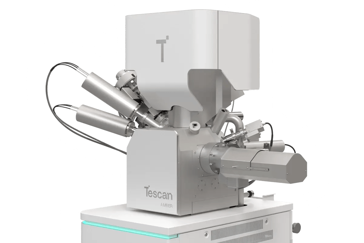
Tescan AMBER 2 with Nanoprototyping Toolbox

Tescan AMBER 2 equips researchers with the speed, precision, and flexibility needed for nanoscale discovery and prototyping. Ultra-high-resolution SEM imaging, FIB milling, and the Nanoprototyping Toolbox come together in one platform—streamlining the path from concept to functional devices.

  • BrightBeam™ UHR SEM: High-resolution, low-kV imaging of sensitive nanostructures

  • Essence™ EBL Kit: Sub-15 nm electron beam lithography with fracture-free PEC and GDSII support

  • Essence™ DrawBeam: Direct-write ion beam milling and deposition for resist-free patterning

  • FIB-SEM Expert PI & VisualCoder: Full automation with Python scripting and visual programming

  • Ultra-fast pattern generator: 20 ns dwell time for high-current lithography and fast exposure

  • Versatile nanofabrication: From 3D spiral resonators to plasmonic sensors, nanowire devices, and AFM probe enhancements


AMBER 2

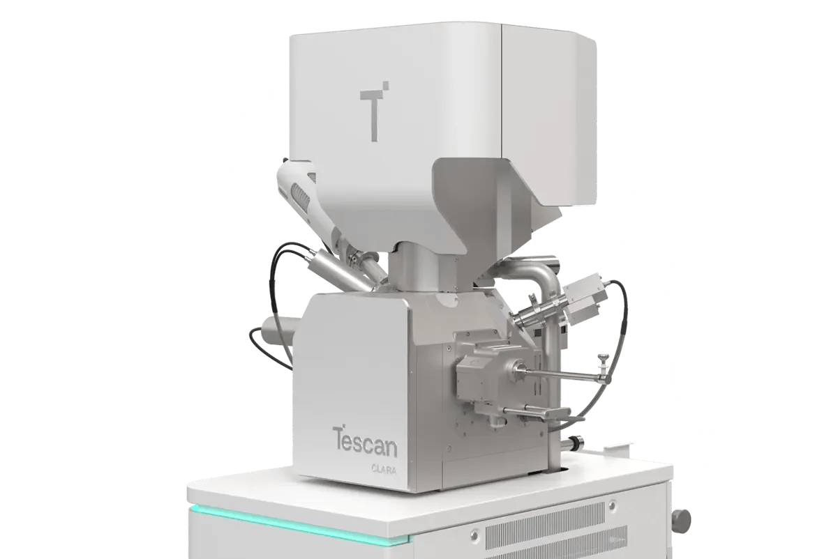
Tescan CLARA  

Tescan CLARA gives you the tools to prototype and analyze nanoscale structures with unmatched precision and flexibility. Ultra-high-resolution SEM imaging, advanced electron beam lithography, and automated scripting combine in one platform—accelerating nanoscale device innovation from concept to functional prototype.

  • BrightBeam™ UHR SEM: Field-free, high-resolution imaging without sample prep

  • Essence™ EBL Kit: Sub-15 nm patterning with PEC and GDSII compatibility

  • Essence™ DrawBeam: Direct-write deposition or gas assisted etching, no resists required

  • FIB-SEM Expert PI & VisualCoder: Full automation via Python scripting and visual programming

  • Ultra-fast pattern generator: 20 ns dwell time and high-current beams for maximum throughput

  • Versatile applications: From plasmonics to biosciences, quantum devices, and AFM probe tuning
CLARA GM Mat. Science

Tescan QuiiN 

Tescan QuiiN delivers precise multi-ion implantation for quantum research and advanced materials engineering. With seamless species selection, in-situ annealing, and single-ion control, it enables defect creation and tuning with unmatched accuracy and repeatability.

  • Unprecedented milling precision: Fine-tune material surfaces with FIB-based implantation

  • Seamless isotope & ion species selection: Switch between N, Ar, O, He, Xe, Au, Ge, Si, or mixtures in one system

  • In-situ annealing up to 950 °C: Repair lattice damage and activate dopants during implantation

  • Precise dose control: Prevent artifacts and ensure uniform implantation results

  • Depth tuning: Control implantation from 3–30 keV for shallow or buried structures

  • Single-ion implantation: Ultra-sensitive current measurement for deterministic doping

Sign up for a personal virtual demo

Our global team is available to answer questions about Tescan solutions for Material Science.

GET IN Touch

GET IN Touch

Contact us

map

Where can you find us:

Tescan
Libušina třída 21
623 00 Brno
Czech Republic

info@Tescan.com