WEBINAR | Up to 40% Faster Automated TEM Lamella Preparation with new Ga⁺ FIB Column

Low-Damage EBSD Sample Preparation with Plasma FIB-SEM and Low Angle Polishing

Prepare deformation-free, large-area surfaces for reliable EBSD analysis, even in complex, multi-phase materials. 

hero
hero
Unlocked content

Why Surface Integrity Affects Crystallographic Accuracy in EBSD Workflows

Electron Backscatter Diffraction (EBSD) requires sample surfaces that are free of deformation and preparation-induced artifacts. Conventional polishing techniques, including mechanical and electrochemical methods, often fall short, especially when working with materials that contain multiple phases.

This application note presents an alternative approach using TESCAN’s Low Angle Polishing method on a plasma FIB-SEM platform. By minimizing surface damage and supporting large-area preparation, this workflow provides consistent, high-quality EBSD results across challenging materials like duplex steel and WC-Co composites.

Why perform EBSD Sample Preparation

with TESCAN?

01
Root of the Problem

Why Deformation-Free Surfaces Are Critical for Reliable EBSD Results

High-quality EBSD analysis relies on undistorted electron backscatter patterns, which are only possible with clean, flat, and deformation-free surfaces. Standard mechanical polishing often removes softer phases unevenly or alters microstructure through heat and strain, while electrochemical techniques are not suitable for all compositions.

These issues limit the accuracy and reproducibility of EBSD data, particularly in multi-phase or beam-sensitive samples commonly encountered in materials research.

02
Materials and Methods

A Plasma FIB-SEM Workflow for Low-Damage EBSD Sample Preparation

Three materials were analyzed: duplex steel and two samples from the WC-Co group. Each was prepared using the TESCAN AMBER X 2 plasma FIB-SEM system, configured with an EBSD camera.

Polishing was performed using TESCAN’s patented Low Angle Polishing method and managed via the Essence™ Low Angle Polishing software module. Ion beam energies varied between 30 keV and 10 keV at different beam currents (30 nA to 100 nA), while EBSD patterns were collected using a 20 keV, 10 nA electron beam.

03
Results and Discussion

High-Quality EBSD Patterns Across Beam Conditions and Sample Types

The Low Angle Polishing workflow produced uniform, artifact-free surfaces suitable for EBSD analysis, even when applied to heterogeneous or hard-to-polish materials. Duplex steel and WC-Co samples exhibited strong, consistent EBSD patterns without evidence of phase transformation or surface distortion.

The ability to polish large areas also enabled broader statistical sampling, improving confidence in orientation and phase distribution results. Automated polishing procedure ensures repeatability, even at higher beam currents—making the method suitable for both research and production settings.

GET IN Touch

Contact us

Get the most out of Tescan

This is more than information; it's an advantage. We've compiled our technical whitepapers, detailed product flyers, and on-demand webinars to provide you with the knowledge that makes a real difference. Sign up now to access the insights you need to make an impact.

Tescan Instruments & Technology

Used in This Workflow

TESCAN AMBER X 2

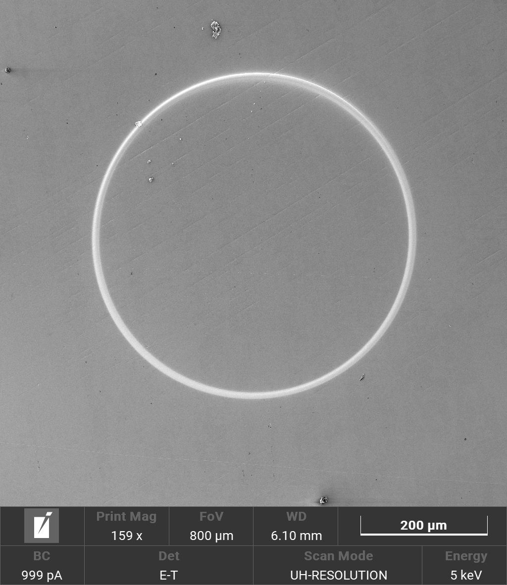
A unique plasma FIB-SEM combining a Xenon plasma FIB with a field-free UHR SEM column, enabling high-throughput milling and high-resolution imaging in one system.

  • Xenon plasma FIB enables Ga-free high-volume milling up to millimeter scale

  • Field-free UHR SEM delivers high-resolution imaging of nanostructures

  • Designed for automated, large-area surface preparation and 3D nanoscale analysis 
AMBER-X 2

GET IN Touch

Contact us

map

Where can you find us:

Tescan Brno
Libušina třída 21
623 00 Brno
Czech Republic

info@Tescan.com