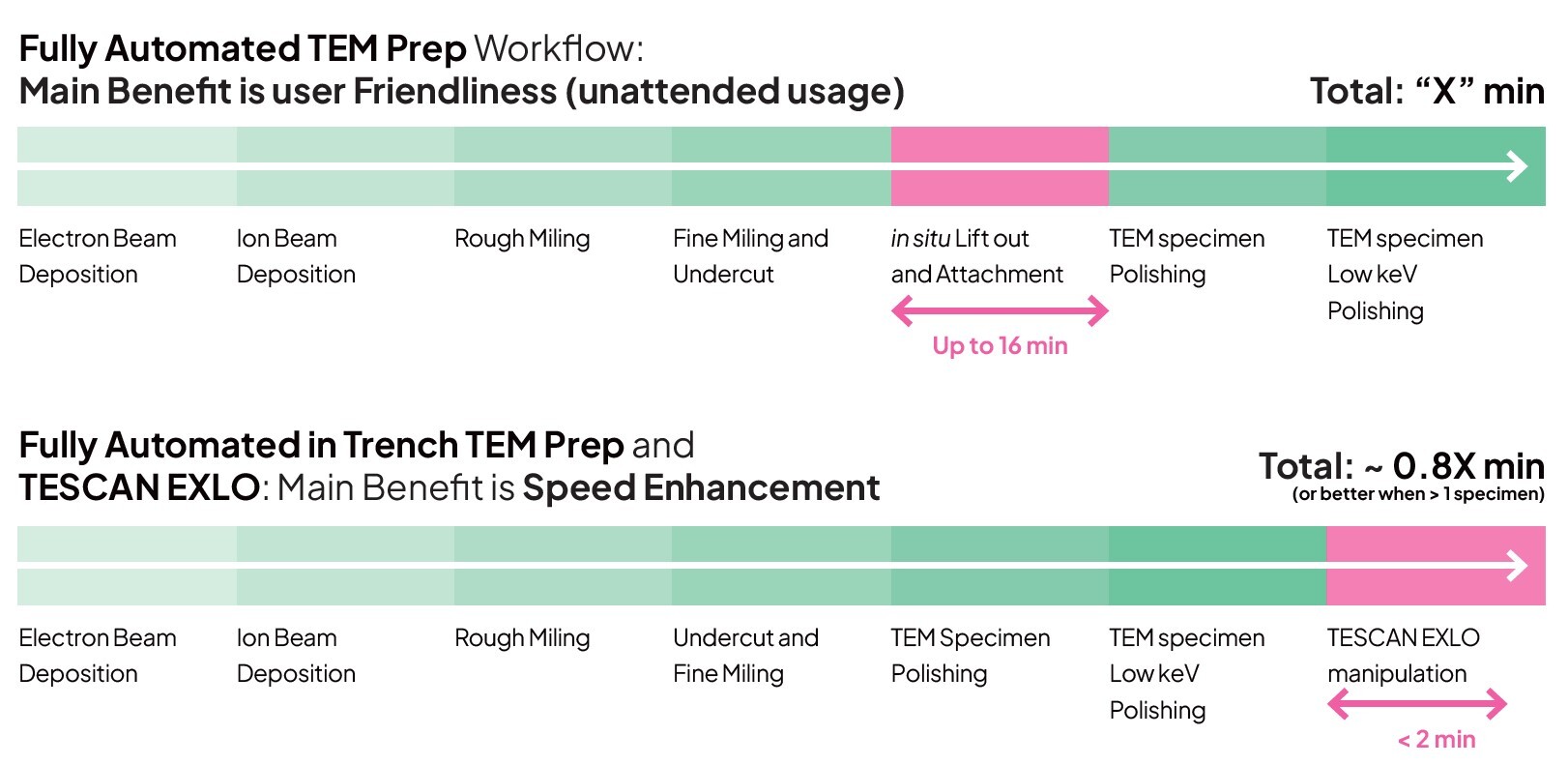
Throughput without Compromise
Increase the number of TEM lamellae per shift by decoupling milling from manipulation.
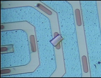
Ex Situ Lift-Out for Scalable, High-Throughput TEM Specimen Preparation

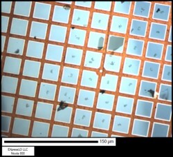
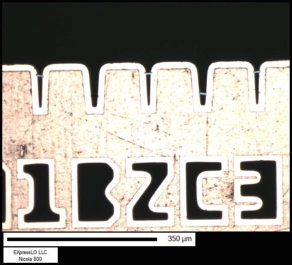
Tescan EXLO™ is designed for laboratories where TEM throughput, reproducibility, and cost efficiency matter. By moving specimen lift-out outside the FIB-SEM, EXLO™ keeps valuable beam time focused on milling, while parallelizing lamella transfer and grid mounting. The result: higher output, lower cost per specimen, and a more efficient workflow.
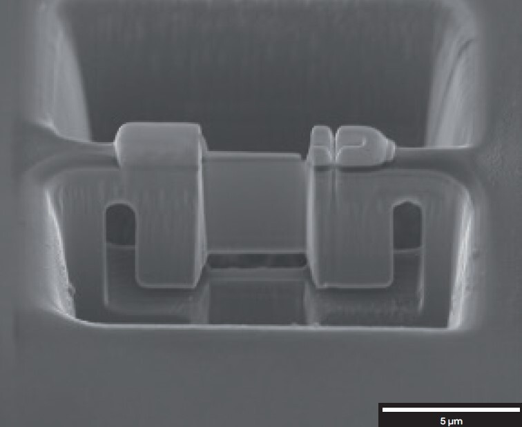
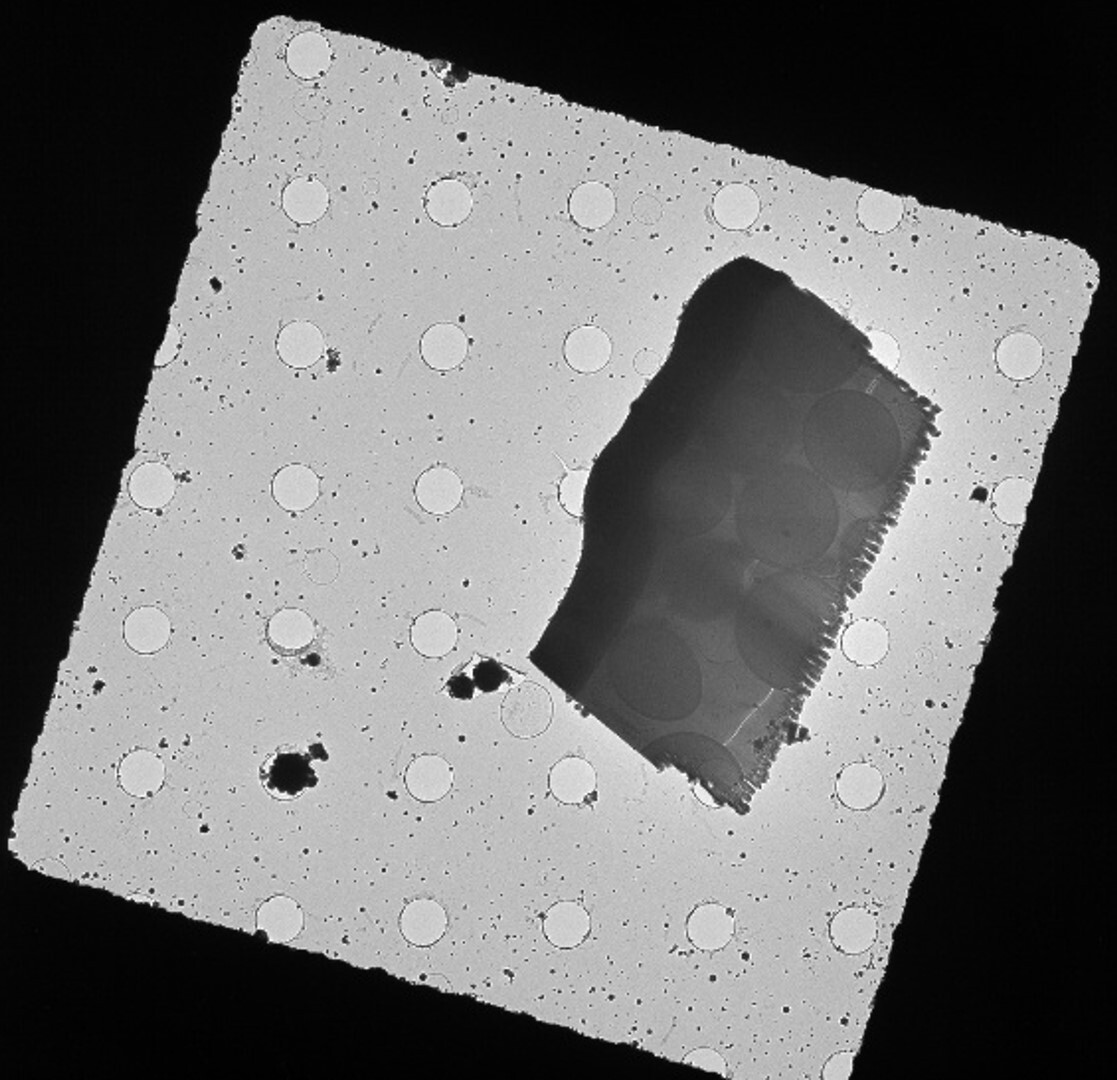
Reliable lift-out for diverse materials and nanostructures
For materials scientists, EXLO™ simplifies the preparation of specimens ranging from thin films to fragile nanostructures. Its precision handling ensures stable transfer and mounting, minimizing artifacts that can affect downstream TEM analysis. With reproducible workflows and optimized grids, EXLO™ enables consistent results for both fundamental research and applied studies.

High-throughput TEM sample preparation for process control and failure analysis
Tescan EXLO™ accelerates semiconductor workflows where specimen demand is high. By decoupling manipulation from FIB usage, engineers can prepare more lamellae per shift without expanding instrument capacity. The system ensures reproducibility across large batches, enabling confident analysis in process development, yield monitoring, and failure diagnostics.

Precise transfer for delicate specimens
EXLO™ provides a controlled environment for preparing specimens that are especially vulnerable to beam damage or contamination. By externalizing the transfer step, researchers can protect the integrity of delicate nanostructures and sensitive materials. This extends the lab’s capabilities into advanced nanotechnology research, ensuring high-quality TEM analysis of even the most delicate specimens.