Master IC Packaging Failure Analysis with Tescan Solutions  


Achieve fast, accurate insight into today’s complex IC packages with Tescan workflows. Gain the precision and reliability to localize defects, validate designs, and accelerate problem-solving across smaller features, advanced materials, and 3D architectures.

Package-Level_Sample_Preparation_for_Failure_Analysis

Tescan solutions

for advanced research in semiconductors
Increase FA Throughput in Challenging Samples Utilizing TRUE X-Sectioning

Combine mask-based plasma FIB milling with Rocking Stage tilting to achieve fast, clean, and repeatable cross sections of complex semiconductor samples. This workflow increases throughput and improves surface quality without the need for coatings or extra polishing.

  • Physical masks: Reshape the beam–sample interaction for high-current milling with fewer artifacts
  • Rocking Stage: Tilts the sample during polishing to reduce curtaining in curved or multi-material regions
  • Versatile workflow: Delivers reliable results across OLEDs, BGAs, MEMS, and TEM lamella
02_1mm-Si-mask-placed-on-the-MLCC-sample_1x
Pair Laser Ablation and Xe Plasma FIB-SEM

Combine femtosecond laser ablation for rapid bulk removal, with precision Xe plasma FIB polishing to achieve fast, accurate, low-damage failure analysis of large and complex semiconductor devices. This hybrid workflow improves throughput and preserves critical structures, from package to nanoscale.

  • Laser ablation: Quickly removes bulk material without mechanical stress or overheating
  • Plasma FIB: Refines surfaces with precise end-pointing and clean polishing for deeper inspection
  • Integrated overlays and CAD alignment: Ensure accurate targeting across tools and samples
2_Laser milling through entire stack of memory dies_1x
Physical Failure Analysis of a MEMS Motion Sensor

Leverage Tescan’s plasma FIB-SEM workflow to create precise, large-area cross sections of MEMS motion sensors without mechanical damage. This approach preserves delicate bonding layers and internal structures while efficiently delivering clear results for accurate failure analysis.

  • Plasma FIB: Avoids mechanical stress to preserve bonding layers and internal structures
  • High-contrast SEM imaging: Reveals metal seams and adhesion interfaces at low kV
  • Wide, artifact-free cross sections: Improve inspection quality while maintaining throughput
3_MEMS contact Plasma FIB cross-sectioning_1x
Prepare Extra-large-area Cross Sections in an OLED Display

Use Tescan’s plasma FIB-SEM workflow to prepare large-area OLED display cross sections up to 1 mm wide. This approach preserves thin-film integrity and reveals critical features for accurate defect localization and interface analysis.

  • High-current plasma FIB milling: Produces deep, uniform trenches without delamination or tearing
  • Low-kV SEM imaging: Reveals clear layer contrast and interface structures across sensitive materials
  • Versatile workflow: Supports failure analysis and process optimization for flexible OLED and Micro-LED displays
06_Micro-LED Plasma FIB cross-section_1x
Rocking Stage for High-quality Polishing of Cross Section Surfaces

Achieve high-quality cross section polishing with TESCAN’s Rocking Stage and real-time, multi-angle plasma FIB milling. This workflow reduces curtaining and improves surface precision in complex semiconductor samples.

  • Alternating tilt: Minimizes curtaining across mixed-material samples without workflow interruptions
  • Continuous SEM observation: Provides precise end-pointing and real-time quality control
  • Large cross sections: Enable faster, more consistent preparation of TSVs, solder bumps, and packaged ICs
1_Flip-chip cross-section surface quality comparison_1x

Tescan Solutions

For Sustainable IC Packaging Analysis

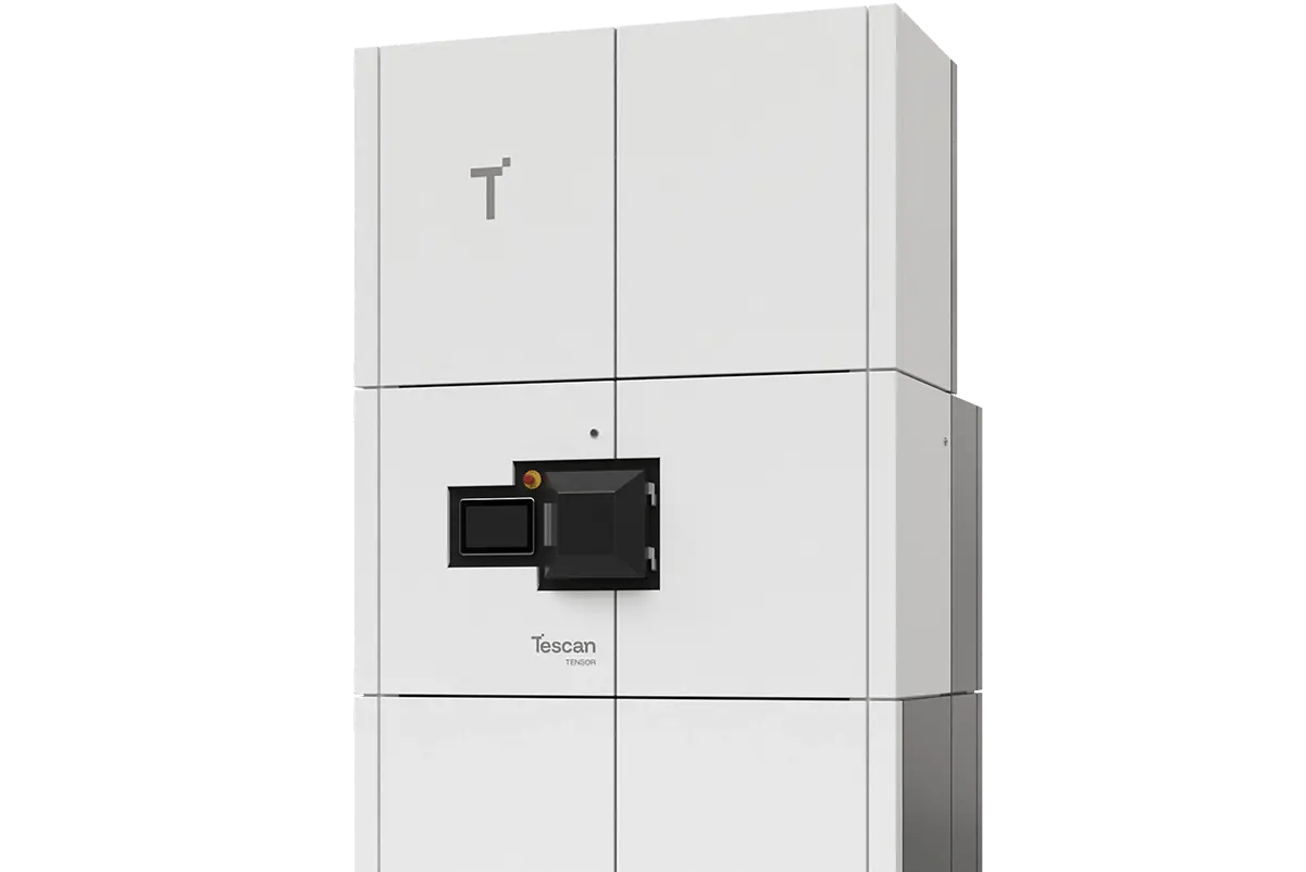
Tescan TENSOR

Tescan TENSOR is an analytical STEM platform for fast, reproducible strain, phase, and composition analysis in semiconductor devices. 

It integrates 4D-STEM, beam precession, and high-throughput EDS to deliver precise nanoscale characterization, with automation that ensures consistent productivity across shifts and sites.

  • Precession-enhanced 4D-STEM: Delivers high-precision strain and phase mapping, even at the 3 nm node

  • Automated workflows: Reduce operator variability with alignments, intuitive interfaces, and real-time data processing

  • Low-dose, high-current operation: Minimizes sample damage and contamination in near-UHV conditions
TENSOR_1

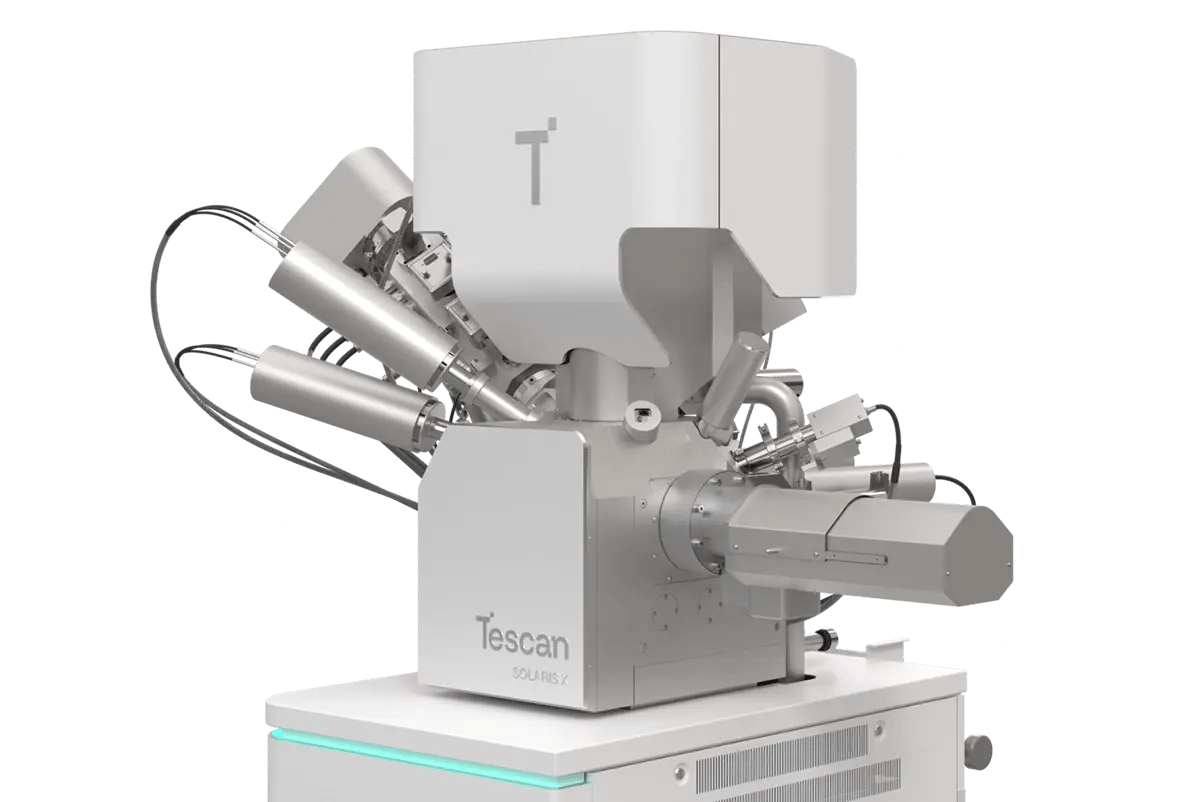
Tescan SOLARIS X2

Tescan SOLARIS X2 is a plasma FIB-SEM for fast, artifact-free cross sectioning and Ga-free sample prep of advanced semiconductor packages. Mistral™ Xe plasma FIB and Triglav™ UHR SEM work together to expose defects and prepare TEM lamellae on one system.

TRUE X-sectioning and Rocking Stage technologies deliver clean, repeatable cross sections across polymers, ceramics, and stacked devices—even at millimeter scale.

  • Live end-pointing with Xe plasma FIB: Accelerates failure localization through deep, clean cross sections of multilayer materials
  • Mistral™ plasma FIB: Provides Ga-free TEM lamella prep with precision comparable to Ga FIBs, freeing capacity from conventional systems
  • Automated workflows: Increase throughput with alignments and optimized switching between preparation and analysis modes
SOLARIS-X2

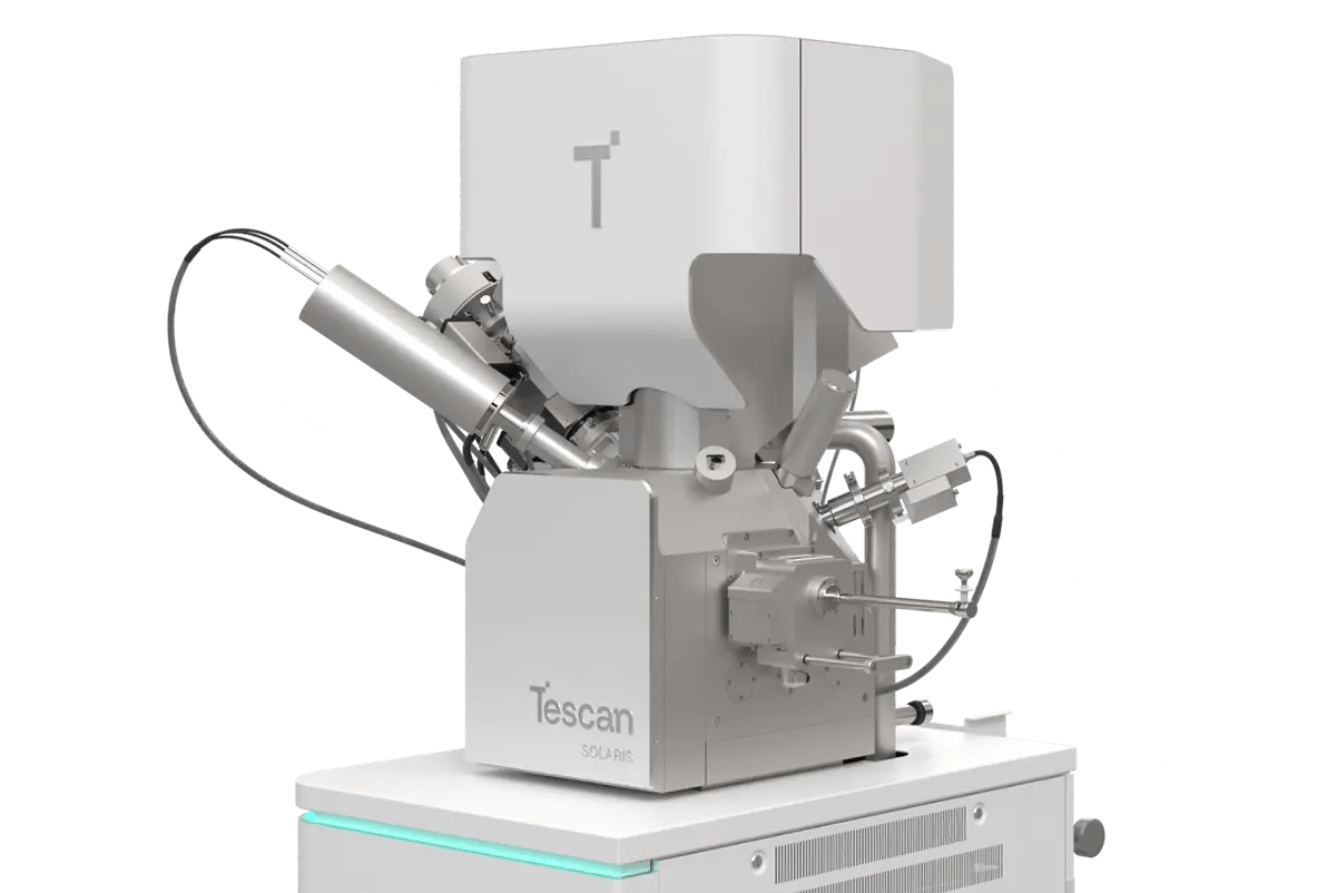
Tescan SOLARIS 2

Tescan SOLARIS 2 is an automated Ga+ FIB-SEM for precise TEM lamella preparation in semiconductor R&D and process control. It integrates Triglav™ SEM, Orage™ Ga FIB, and AutoTEM Pro™ software to produce ultra-thin lamellae from sub-10 nm nodes.

Designed for 24/7 operation, it supports planar, top-down, and inverted workflows with minimal training, ensuring consistent results across users and shifts.

  • AI-guided workflows: Produce ultra-thin (<50 nm) TEM specimens with real-time end-pointing
  • Automated sequences: Run unattended prep, including overnight alignments and batch processing
  • Reproducible outcomes: Minimize manual steps to increase throughput in advanced TEM workflows
SOLARIS X

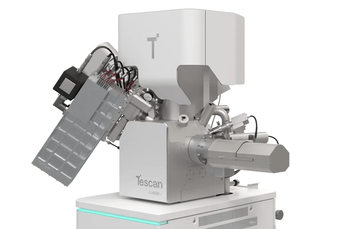
Tescan AMBER X2

Tescan AMBER X2 is a versatile plasma FIB-SEM for damage-free delayering and in-situ probing of advanced ICs. It delivers automated, repeatable workflows with sub-10 nm targeting precision, combining Mistral™ Xe plasma FIB and BrightBeam™ SEM for high-resolution imaging and fault localization with minimal rework.

  • Recipe-driven delayering: Streamlines fault isolation with optimized contrast for structure recognition
  • Xe ion beam with tailored chemistries: Provides uniform, artifact-free layer removal down to 500 eV
  • Integrated platform: Combines delayering, probing, and imaging in one tool to reduce handoffs and operator time
AMBER-X2

Sign up for a personal virtual demo

Our global team is available to answer questions about Tescan solutions for Semiconductors.

GET IN Touch

Contact us

map

Where can you find us:

Tescan Brno
Libušina třída 21
623 00 Brno
Czech Republic

info@Tescan.com