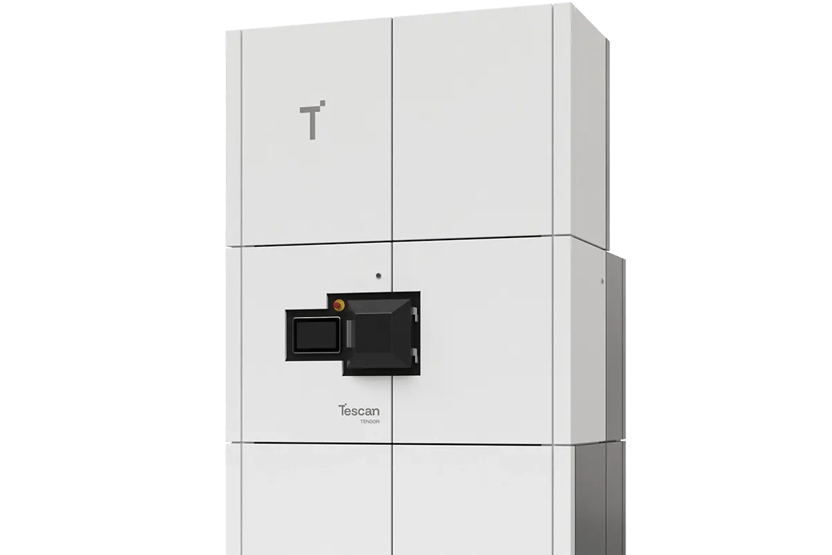
WEBINAR | Dynamic-to-Detail Micro-CT in One Workflow: UniTOM HR 2

Gain Clarity for Faster Process Development with Reliable Multimodal STEM Workflows 


Accelerate process development with real-time phase and orientation mapping. Get clear insight into nanoscale structures to guide decisions with speed and confidence.

Metrology_and_Process_development

Tescan solutions

for advanced research in semiconductors
2D-Strain Analysis in Semiconductor Devices: A Case Study of 5-nm FinFET Circuits

Tescan TENSOR can perform precise strain measurements across large sample areas in complex semiconductor devices, such as 5-nm FinFET circuits or GAA nanosheets.

The precise beam-precession alignments, unrestricted speed of data acquisition, and proprietary strain calculation algorithm ensure high accuracy and precision, helping optimize strain engineering and improve device performance.

Grain Size Distribution in Multiphase Nanodevices: A Case Study in 3D-NAND Devices
Tescan TENSOR simplifies grain size distribution analysis in complex, multiphase devices. Its fast beam precession and real-time data processing enable rapid, accurate determination of phase and grain structure across large regions of stacked VNAND devices, delivering results in a fraction of the time in comparison with the traditional TEM/STEM instruments.
Routine Characterization of Semiconductor Devices: A Case Study of 3D NAND Cells

Tescan TENSOR’s windowless EDS detectors, combined with high beam currents and 100 kV acceleration, produce strong signals even for light elements such as carbon, nitrogen, and oxygen. This capability is particularly beneficial for small devices like 3D NAND cells.  

The EDS analysis can be further augmented by 4D-STEM phase and orientation mapping (ACOM), which integrates seamlessly into the system’s automated workflows, allowing for enhanced characterization with minimal user effort. 

Routine Characterization of Semiconductor Devices: A Case Study of 22-nm S/D Node

TENSOR provides high-quality EDS data using its dual 100 mm² detectors placed near the sample, enabling a total collection solid angle of 2.0 sr. With 100 keV energy and electron beam currents up to 10 nA at a 1 nm beam size, EDS maps are captured in just minutes, as opposed to the typical half-hour.

Additionally, Tescan TENSOR’s rapid switching between STEM imaging and EDS mapping without manual alignments enhances throughput in these routine measurements.

Enhancing Failure Analysis with 4D-STEM: A Case Study of Phase Change Memory

For advanced semiconductor devices like phase change memory modules, Tescan TENSOR enables precise structural failure analysis.

By unambiguously identifying defects such as germanium separation or amorphization in layers and vias, you can diagnose and address failure points with confidence.

Fast 4D-STEM Phase Mapping for PCM Devices

Combine Tescan’s 4D-STEM workflow with integrated beam precession to achieve fast, accurate phase and orientation mapping in semiconductor devices. Structural insights are delivered in under 15 minutes, supporting both failure analysis and process optimization.

  • Precession-assisted 4D-STEM: Minimizes dynamical effects and captures crystalline, amorphous, and mixed-phase regions in a single scan
  • Real-time mapping: Provides immediate results with automated cross-correlation and no manual tuning
  • High-throughput analysis: Reveals structural changes in materials like PCM for reliable process development
Figure 2_1x-1

Tescan Solutions

for Metrology and Process Development

Tescan TENSOR

Tescan TENSOR is an analytical STEM platform for fast, reproducible strain, phase, and composition analysis of semiconductor devices.

It integrates 4D-STEM, beam precession, and high-throughput EDS to deliver precise nanoscale structural and elemental characterization. Optimized for automation and consistency, TENSOR ensures high productivity across shifts and sites.

  • Precession-enhanced 4D-STEM: Provides high-precision strain and phase mapping, even at the 3 nm node

  • Automated alignments and workflows: Reduce operator variability with real-time data processing

  • Low-dose, high-current operation: Minimizes sample damage and contamination in near-UHV conditions
TENSOR_1

Sign up

Book a demo

Built around your needs

map

Where can you find us:

Tescan
Libušina třída 21
623 00 Brno
Czech Republic

130405923 us US 37.09024 -95.712891 25.3575 29.349345 20.67957527 42.082797 39.91384763 -33.693421 13.93320106 3.039986586 31.997988 38.050985 47.579533 48.1485965 58.375799 54.663142 19.195447 56.975106 50.493053 45.868592 10.79556993 44.35660598 43.2371604 55.536415 14.557577179752773 32.100937 -6.116829 -6.212299277967318 23.7104 -33.471062 31.998740087 -23.69149395 43.462349 51.529848 49.1893523 49.197486 25.072375 31.075811 1.299027 40.676979 52.30150662 51.013813 35.684121 37.479653 52.246622 40.581349 39.911632 -26.1811371 41.818215 33.429928 -12.08688

No distributors found.