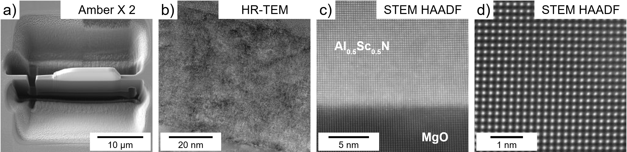
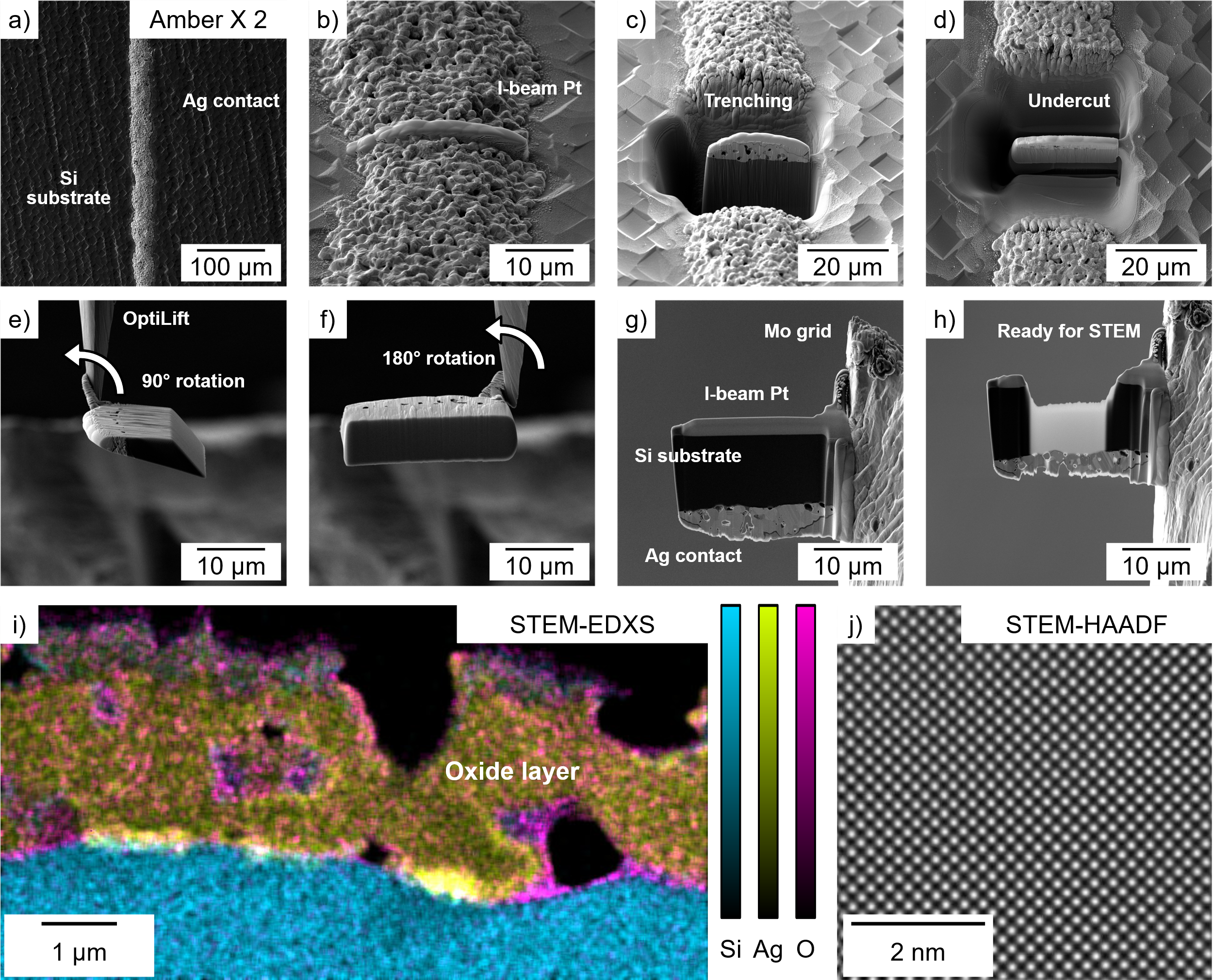
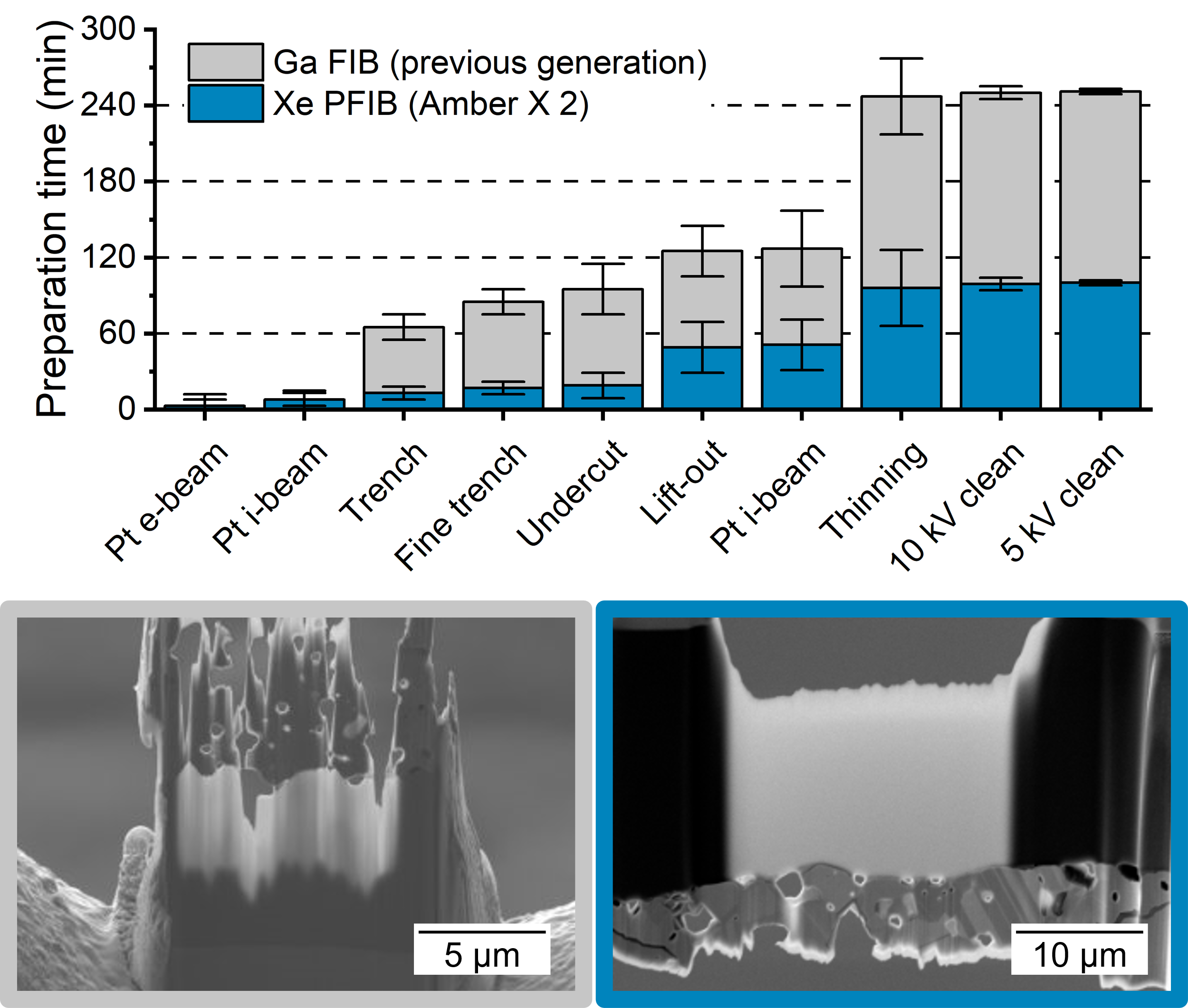
WEBINAR | Up to 40% Faster Automated TEM Lamella Preparation with new Ga⁺ FIB Column

Perform TEM Sample Preparation Without Ion Implantation Using Tescan AMBER X 2 

Enhance TEM sample preparation with Tescan AMBER X 2 to reliably produce ultra-thin lamellae free from ion implantation artifacts.

hero
hero
Unlocked content

Enable TEM Sample Preparation That Preserves Atomic Structure and Minimizes Ion Implantation

High-resolution TEM and APT require ultra-thin, electron-transparent samples where atomic detail is preserved. Conventional Ga FIB preparation often causes gallium implantation, amorphization, and artifacts that limit imaging accuracy. Thin films, grain boundaries, and semiconductor interfaces are especially prone to beam-induced damage.

Tescan AMBER X 2 uses Xe plasma FIB with the Mistral™ column to enable low-damage TEM sample preparation. Create high-quality lamellae and atom probe tips with minimized implantation and preserved structure. Prepare site-specific regions across insulating substrates, porous layers, and nanoscale interfaces with speed, precision, and reliability.  

Why Perform TEM Sample Preparation

with Plasma FIB-SEM on TESCAN AMBER X 2?

01
Root of the Problem

Why Standard FIB Preparation Fails in TEM Sample Preparation

Preparing high-quality TEM samples requires ultra-thin, electron-transparent lamellae where structural and chemical details remain intact. Conventional Ga FIB techniques often introduce gallium implantation, amorphization, or surface contamination that obscure true material features. Sensitive regions such as thin films, grain boundaries, and semiconductor interfaces are particularly prone to beam damage.

Even minor implantation or amorphization can distort lattice information, compromise spectroscopy, or mask defects at the nanoscale. This limits the reliability of both imaging and analysis in advanced materials research.

TESCAN AMBER X 2 addresses these challenges with a plasma FIB-SEM workflow optimized for high-quality TEM sample preparation.

  • Xe plasma FIB reduces ion implantation and amorphization
  • Wide beam current range enables both fast milling and fine thinning
  • High-resolution Mistral™ column preserves structural fidelity

02
Materials and Methods

How TEM Samples Were Prepared Using TESCAN AMBER X 2 Plasma FIB-SEM

A nitride thin film on an insulating substrate was selected to demonstrate site-specific TEM sample preparation. The region of interest was identified using high-resolution SEM imaging at low kV to ensure precise targeting of the interface.

Lamella preparation was performed with the Xe plasma FIB at 30 keV using a wide current range, enabling both efficient bulk milling and controlled thinning. A protective Pt layer was deposited before milling to safeguard the surface. Final polishing at low kV minimized amorphization and preserved lattice detail.

This workflow produced electron-transparent lamellae with minimal implantation and artifact-free interfaces, suitable for atomic-scale imaging and microstructural analysis.

03
Results and Discussion

TESCAN AMBER X 2 enabled reliable preparation of electron-transparent lamellae for high-resolution TEM and APT analysis. Xe plasma milling preserved structural integrity while minimizing ion implantation and amorphization across sensitive interfaces.

SEM inspection confirmed well-defined boundaries in nitride thin films, grain interfaces, and insulating substrates. Low-kV imaging delivered strong contrast for assessing defects, voids, and interfacial quality. Protective Pt layers and final low-kV polishing ensured lattice detail was retained without surface contamination.

Prepared lamellae exhibited uniform thickness, intact crystallinity, and stable geometry across challenging materials. Even in beam-sensitive regions, structural fidelity was preserved. This workflow delivers high-quality samples for atomic-scale imaging, chemical mapping, and microstructural investigations in advanced materials research.

Common Challenges in High-Resolution Material Analysis

Advanced materials used in energy storage, aerospace, nanotechnology, and biomedical applications require in-depth structural insights. However, traditional imaging techniques often fall short when analyzing multi-phase structures, nanoscale defects, and buried interfaces.

FIB-SEM tomography addresses these challenges by providing:
  • Sub-nanometer precision in 3D imaging for detailed microstructural analysis.
  • Site-specific cross-sectioning to study buried features without sample destruction.
  • Multi-modal integration with EDS and EBSD for correlative material characterization.

TEM Sample Preparation for Atomic-Scale 

Imaging and Microstructural Analysis 
Using High-Resolution (S)TEM with 
TESCAN AMBER X 2 Plasma FIB-SEM

GET IN Touch

Contact us

Get the most out of Tescan

This is more than information; it's an advantage. We've compiled our technical whitepapers, detailed product flyers, and on-demand webinars to provide you with the knowledge that makes a real difference. Sign up now to access the insights you need to make an impact.

Tescan Instruments & Technology

Used in This Workflow

Tescan AMBER X 2

Tescan AMBER X 2 delivers the precision and throughput required for high-quality TEM and APT sample preparation while minimizing ion implantation and amorphization.

With its Xe plasma source and Mistral™ FIB column design, AMBER X 2 combines high-current milling for rapid material removal with fine beam resolution close to Ga FIB systems—preserving structural fidelity across sensitive materials.

  • Xe plasma FIB: fast, non-reactive milling with minimal contamination
  • Mistral™ FIB column: sharp beam profile for accurate thinning and polishing
  • Wide current range: supports both bulk trenching and nanometer-scale finishing
  • Integrated high-resolution SEM: ensures precise targeting and inspection
  • Low-kV final polishing: reduces amorphization and maintains lattice detail
  • Automation options: enable repeatable, site-specific sample preparation for advanced workflows
AMBER-X 2

GET IN Touch

Contact us

map

Where can you find us:

Tescan Brno
Libušina třída 21
623 00 Brno
Czech Republic

info@Tescan.com