WEBINAR | Dynamic-to-Detail Micro-CT in One Workflow: UniTOM HR 2

Achieve Consistent 80 nm Lamella for DRAM Failure Analysis with TESCAN’s Xe FIB-SEM  

Use Tescan SOLARIS X 2 with Mistral™ Xe plasma FIB for TEM sample preparation of SDRAM devices. Produce thin, Ga-free lamellae that preserve interface quality and elemental contrast at the 66 nm node.

5-3_TEM specimen prepared from a 66 nm SDRAM sample using TESCAN SOLARIS X Xe plasma FIB-SEM
5-3_TEM specimen prepared from a 66 nm SDRAM sample using TESCAN SOLARIS X Xe plasma FIB-SEM-mobile
Unlocked content

Resolve Ti and Oxide Interfaces in TEM with Xe Plasma FIB-SEM Sample Preparation

SDRAM devices at the 66 nm node feature delicate multilayer stacks where Ti and oxide interfaces must remain intact for accurate failure analysis. Ga FIB prep methods often cause amorphization or ion implantation, which can distort elemental signals and mask structural details critical to root cause evaluation.

Tescan SOLARIS X with iFIB+™ Xe plasma FIB provides a clean, Ga-free alternative for preparing thin lamellae suitable for TEM and EDS. Maintain interface integrity, reduce damage, and produce reliable TEM specimens for confident analysis of sub-100 nm DRAM structures. 

Why Prepare TEM Lamellae from SDRAM Devices

using Tescan SOLARIS X with Xe Plasma FIB?

01
Root of the Problem

Why Ga-Based FIB Prep Compromises DRAM Failure Analysis

Sub-100 nm DRAM devices contain delicate gate and capacitor structures that demand precise, low-damage TEM preparation. However, Ga FIB workflows often introduce amorphous damage, ion implantation, and redeposition — particularly in sensitive regions like Ti contacts and oxide interfaces.

These effects degrade image contrast, interfere with EDS signals, and reduce confidence in failure analysis results.

Tescan SOLARIS X with iFIB+™ Xe plasma FIB avoids these limitations by combining inert ion milling with fine beam control and in-situ monitoring.

  • Ga-free prep preserves native material chemistry
  • Final thinning below 5 keV reduces amorphous surface layers
  • Real-time SEM imaging supports immediate lamella QC
  • Compatible with BF-STEM, HAADF, and EDS mapping

Avoid rework, reduce artifacts, and confidently localize failures in lamellae prepared from today’s most advanced DRAM technologies. 

02
Materials and Methods

How TEM Sample Preparation Was Performed Using Tescan SOLARIS X with Xe Plasma FIB-SEM

A 66 nm SDRAM sample was selected to demonstrate the effectiveness of non-Ga FIB TEM lamella preparation using the Tescan SOLARIS X. The region of interest was first identified with high-resolution SEM imaging to localize gate-level structures and capacitor arrays.

Bulk trenching and lamella lift-out were performed using high-current Xe plasma milling, followed by stepwise thinning to achieve electron transparency. Final thinning was carried out below 5 keV to minimize amorphous damage and preserve critical interface quality.

Lamella quality was verified in-situ using SEM contrast and geometric inspection. The completed sample was mounted ex-situ and imaged using BF-STEM and HAADF detectors. EDS mapping was used to confirm oxide and Ti layer integrity across the thinned region.

The Xe FIB-SEM workflow ensured fast, repeatable, and contamination-free preparation of high-quality TEM specimens from targeted DRAM structures.

03
Results and Discussion

Produce High-Quality Lamella for STEM and EDS Analysis of DRAM Interfaces

Using Tescan SOLARIS X with Xe plasma FIB, a lamella approximately 80 nm thick was prepared from the active region of a 66 nm SDRAM device. In-situ SEM imaging confirmed uniform thinning and edge integrity prior to lift-out.

Post-preparation imaging in BF-STEM and HAADF modes revealed clear resolution of gate structures, dielectric layers, and capacitor contacts. Interface contrast remained high across oxide and Ti regions, with minimal surface damage or curtaining.

EDS mapping confirmed the presence and spatial continuity of key materials, including Ti electrodes and adjacent oxide layers. Spectral data showed no evidence of Ga contamination, supporting the inert milling characteristics of the Xe source. 

Together, the results demonstrate that the SOLARIS X workflow delivers electron-transparent lamellae suitable for advanced DRAM failure analysis — with reliable structure preservation, strong elemental contrast, and efficient prep time.

GET IN Touch

Contact us

Get the most out of Tescan

This is more than information; it's an advantage. We've compiled our technical whitepapers, detailed product flyers, and on-demand webinars to provide you with the knowledge that makes a real difference. Sign up now to access the insights you need to make an impact.

Tescan Instruments & Technology

Used in This Workflow

Tescan SOLARIS X 2 with Mistral™ Xe Plasma FIB: Versatile, User-friendly FIB-SEM platform 
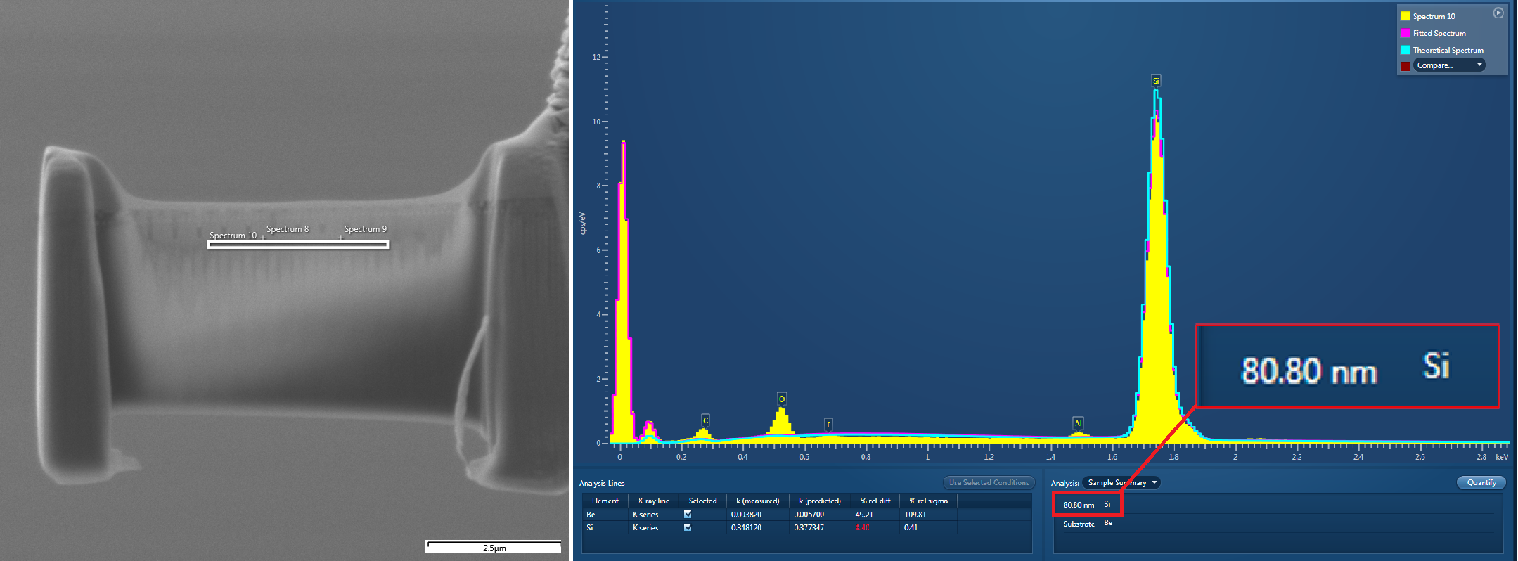
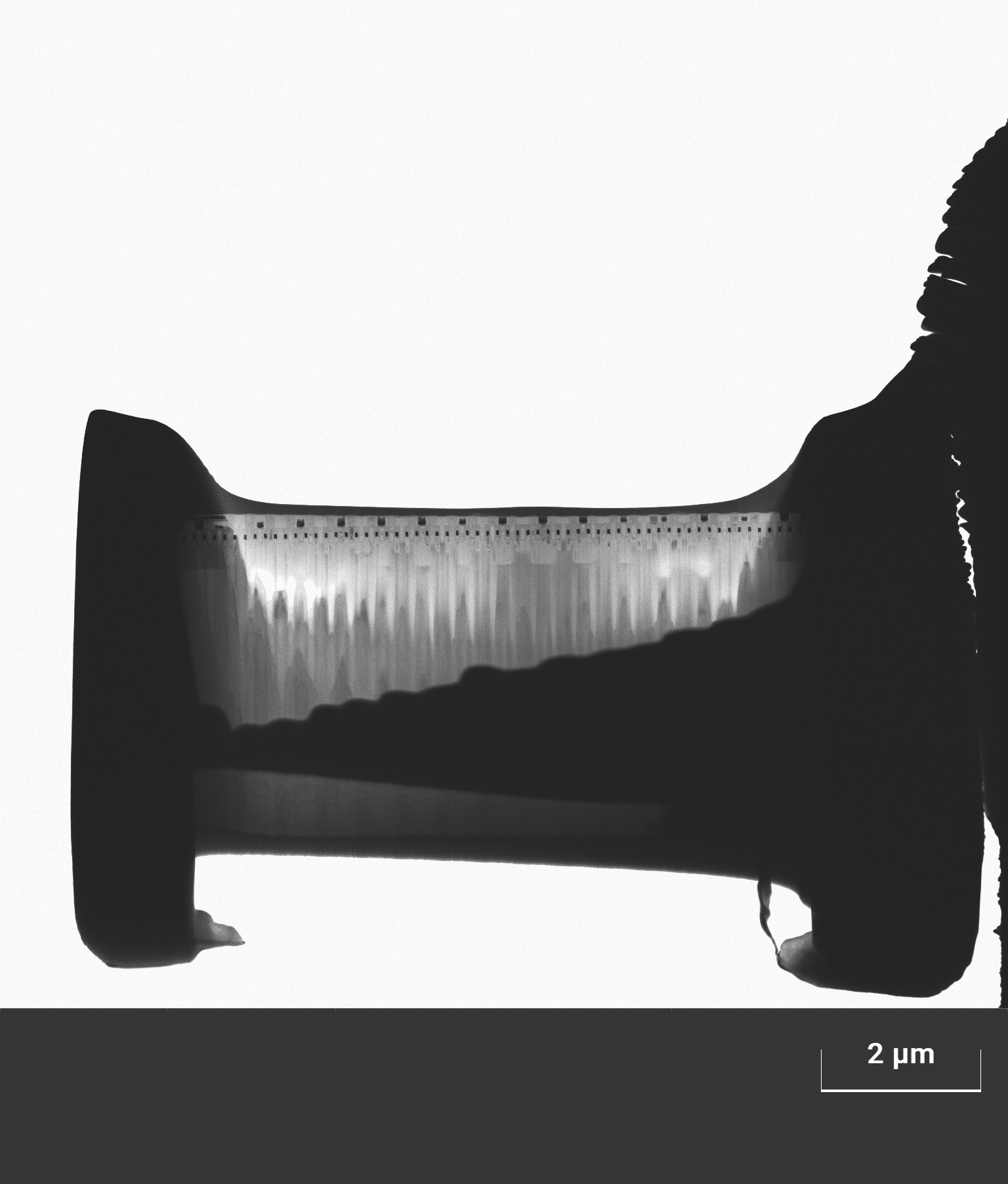
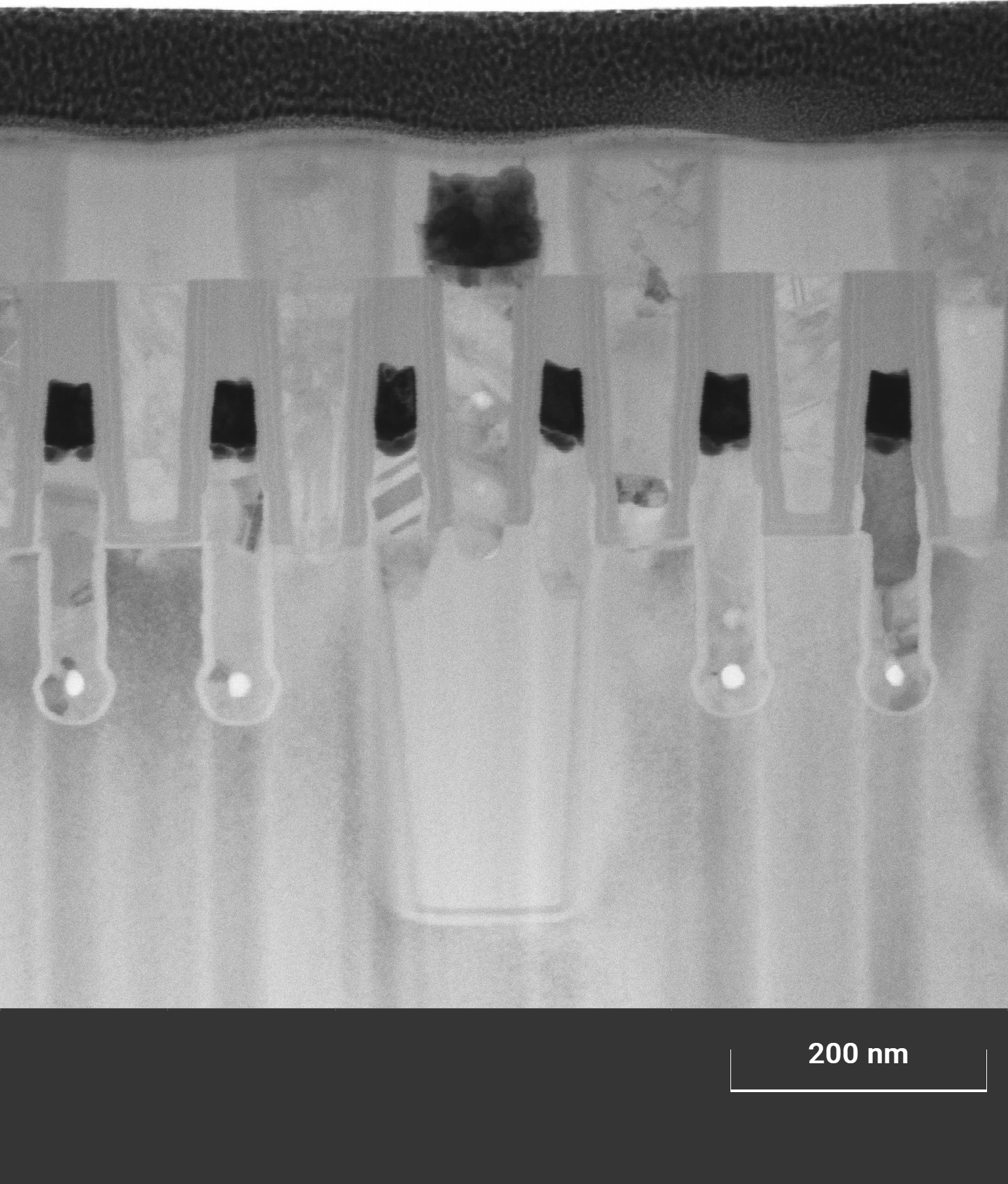
Tescan SOLARIS X 2 delivers fast, high-current Xe plasma FIB milling and precise low-current thinning, ensuring optimal thickness and structure preservation. Its inert Xe ion source enables clean lamella preparation for advanced semiconductor failure analysis without the contamination that occurs with gallium FIB sample preparation.

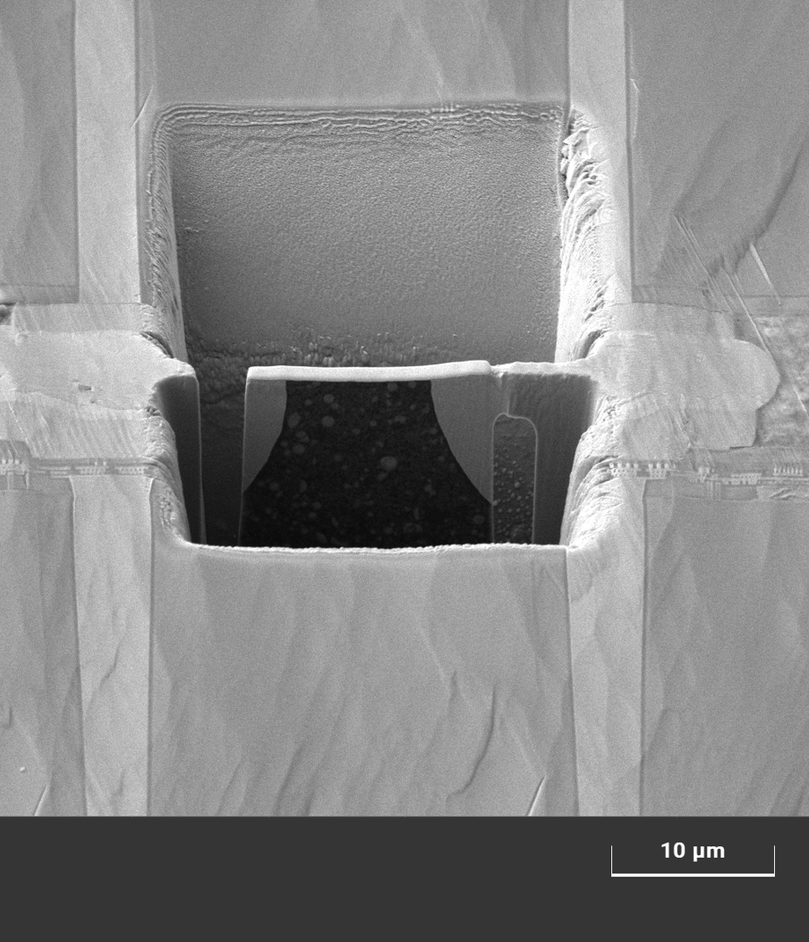
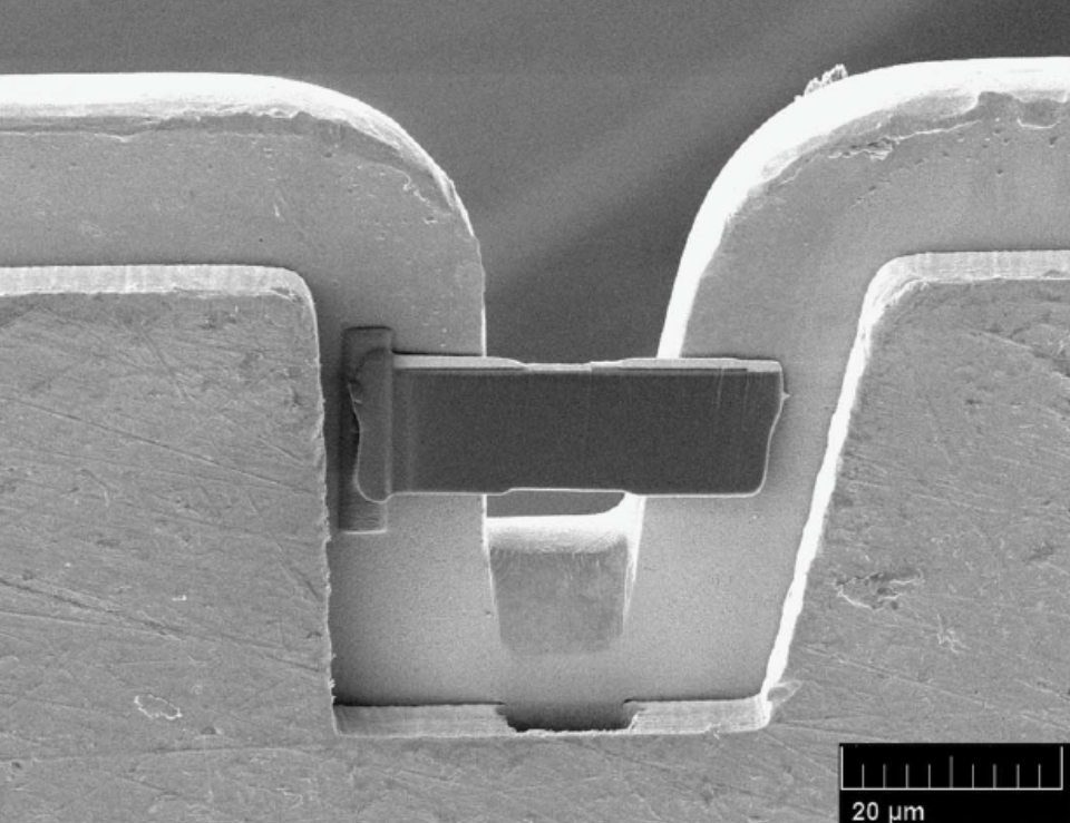
High resolution SEM imaging enables locating regions of interest, monitoring sample thinning in real-time and inspecting final thinned samples to verify compatibility with downstream STEM and EDS workflows. Mistral™ Xe Plasma Column: supports fast bulk milling and delicate lamella thinning

  • Inert ion beam avoids chemical artifacts and eliminates gallium implantation that occurs with traditional Ga+ FIB sample preparation
  • Final thinning below 5 keV: minimizes amorphous damage at critical interfaces
  • Real-time SEM imaging: enables pre-liftout lamella QC
  • Wide range of beam currents enable both speed and precision in one system
SOLARIS-X2

GET IN Touch

Contact us

map

Where can you find us:

Tescan
Libušina třída 21
623 00 Brno 
Czech Republic

info@Tescan.com 

130405923 us US 37.09024 -95.712891 25.3575 29.349345 20.67957527 42.082797 39.91384763 -33.693421 13.93320106 3.039986586 31.997988 38.050985 47.579533 48.1485965 58.375799 54.663142 19.195447 56.975106 50.493053 45.868592 10.79556993 44.35660598 43.2371604 55.536415 14.557577179752773 32.100937 -6.116829 -6.212299277967318 23.7104 -33.471062 31.998740087 -23.69149395 43.462349 51.529848 49.1893523 49.197486 25.072375 31.075811 1.299027 40.676979 52.30150662 51.013813 35.684121 37.479653 52.246622 40.581349 39.911632 -26.1811371 41.818215 33.429928 -12.08688

No distributors found.