WEBINAR | Dynamic-to-Detail Micro-CT in One Workflow: UniTOM HR 2

Achieve <10 nm TEM Lamella from FinFET Devices with TESCAN SOLARIS 2  

Prepare sub-10 nm TEM lamella from FinFET gate and fin regions using Tescan SOLARIS 2 — with the precision needed to maintain structural integrity and spatial accuracy.

5-2_TEM sample preparation from a 10nm FinFET device
5-2_TEM sample preparation from a 10nm FinFET device-mobile
Unlocked content

Extract Sub-10 nm TEM Lamella from FinFET Gate and Fin Regions for Precise Structural Analysis

Advanced node FinFET devices contain complex 3D gate and fin architectures, often buried beneath multiple metal and dielectric layers. Preparing TEM lamella from these regions requires nanometer-level accuracy to preserve structure and avoid damage during thinning.

Tescan SOLARIS 2 combines precise Ga+ FIB milling with low-keV SEM end-pointing to deliver consistently high quality, sub-10 nm lamella from site-specific regions. Extract gate-cut or fin-cut samples, maintain structural integrity, and achieve the dimensional control needed for reliable TEM analysis of 10 nm FinFET devices. 

Why Prepare TEM Lamella from FinFET Devices

with TESCAN SOLARIS FIB-SEM

01
Root of the Problem

Why Standard TEM Prep Workflows Fall Short on 10 nm FinFET Devices

Preparing high-quality TEM lamella from 10 nm FinFET structures demands extreme precision. Yet standard FIB-SEM workflows often struggle to meet these requirements. Thinning below 10 nm without damaging gate or fin features is technically challenging, especially when sample handling, beam damage, or curtaining disrupt the process.

FinFET gate and fin structures are small, buried, and geometrically complex. Even minor misalignment during trenching or lift-out can obscure critical interfaces or cause lamella distortion. And final thinning steps often introduce amorphization that degrades TEM resolution.

Tescan SOLARIS 2 addresses these challenges with a finely tuned, application-focused approach to TEM sample prep.

  • In-situ lift-out minimizes contamination and mechanical stress
  • Inverted geometry supports lamella stability during thinning
  • SEM end-pointing enables accurate targeting of gate and fin regions
  • 1 keV final FIB polish removes damage layers while preserving structure
  • Reliable results across both gate-cut and fin-cut configurations

Extracting sub-10 nm lamella from FinFET devices no longer needs to be a bottleneck. With SOLARIS 2, you gain a reliable, repeatable path to clean, TEM-ready samples.

02
Materials and Methods

How TEM Lamella Were Prepared from FinFET Devices Using TESCAN SOLARIS 2 FIB-SEM

A 10 nm FinFET device was selected to demonstrate routine TEM lamella preparation. The region of interest was located using high-resolution SEM imaging with a 2 keV in-beam secondary electron detector to ensure accurate targeting of gate and fin structures.

Trench milling and sample thinning were performed using the Orage™ Ga+ FIB column, with Pt protection deposited before lift-out. The lamella was extracted in-situ using a nanomanipulator and attached directly to a TEM grid for final thinning.

An inverted geometry was used to improve mechanical stability and minimize curtaining during polishing. Final FIB cleaning at 1 keV ensured sub-10 nm lamella thickness while preserving structural integrity at material interfaces.

This workflow enabled reliable preparation of both gate-cut and fin-cut samples, suitable for high-resolution cross-sectional TEM analysis without structural distortion or contamination.

03
Results and Discussion

High-Resolution TEM Analysis of Gate and Fin Structures in FinFET Devices

Tescan SOLARIS 2 FIB-SEM enabled consistent preparation of sub-10 nm lamella from both gate-cut and fin-cut regions of a 10 nm FinFET device. Inverted geometry combined with low-keV polishing preserved the structural integrity of metal, dielectric, and semiconductor layers across the lamella.

TEM imaging revealed crisp interfaces and minimal amorphous damage, allowing for clear visualization of gate architecture, fin contours, and interconnect structures. The quality of thinning enabled analysis of critical features such as contact spacing, channel uniformity, and interface quality.

Gate regions displayed well-preserved poly-Si and high-k stack structures, while fin-cut lamella provided high-contrast views of fin pitch, oxide boundaries, and diffusion layers. Cross-sectional images confirmed uniform lamella thickness and precise feature retention across samples.

This workflow proved to be a reliable path for device-level failure analysis, structural validation, and process insight at the 10 nm technology node. It delivered the precision and consistency engineers need to push semiconductor development forward with confidence.

GET IN Touch

Contact us

Get the most out of Tescan

This is more than information; it's an advantage. We've compiled our technical whitepapers, detailed product flyers, and on-demand webinars to provide you with the knowledge that makes a real difference. Sign up now to access the insights you need to make an impact.

Tescan Instruments & Technology

Used in This Workflow

TESCAN SOLARIS 2 FIB-SEM 

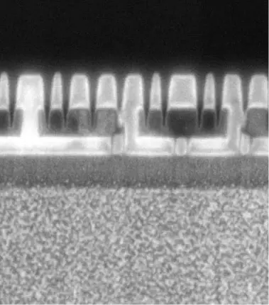
Tescan SOLARIS 2 FIB-SEM delivers the precision, stability, and imaging performance required for advanced TEM lamella workflows on 10 nm FinFET devices.

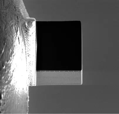
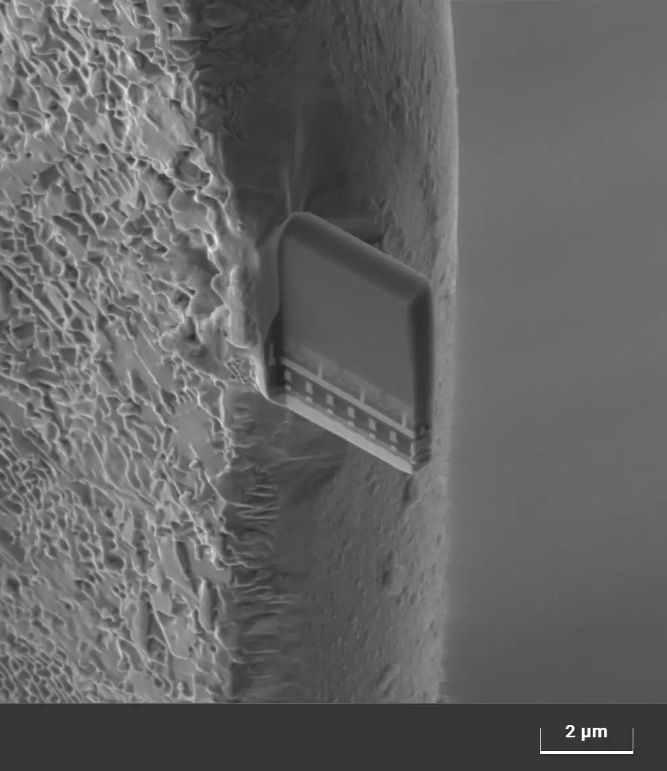
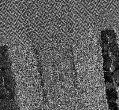
It integrates high-resolution SEM imaging with controlled Ga FIB milling, enabling site-specific preparation of sub-10 nm samples without compromising structure.

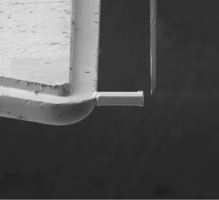
You can prepare both gate-cut and fin-cut lamella with confidence, using in-situ lift-out, inverted geometry, and low-keV thinning to achieve optimal quality and consistency.

  • Integrated SEM and Ga FIB platform: supports full trenching, lift-out, and thinning workflows on a single system

  • In-situ lift-out capabilities: minimize contamination and reduce handling risks during TEM sample transfer

  • Sub-10 nm lamella preparation: ensures dimensional accuracy for high-resolution TEM analysis

  • Optimized workflow stability: allows for reproducible sample prep across FinFET devices

  • Application-tuned system control: supports inverted geometry and precise polishing routines
SOLARIS X

Triglav™ SEM Column 

The Triglav™ SEM column provides stable, high-resolution imaging at low keV, crucial for precise end-pointing during TEM lamella thinning.

Low landing energy operation reduces charging and beam damage, enabling detailed imaging of buried FinFET features throughout the thinning process.

  • High-resolution low-keV imaging: enables precise end-pointing down to gate and fin interfaces
  • 2 keV in-beam SE detection: delivers clear surface contrast with minimal beam-induced damage
  • Stable column alignment: ensures consistent image quality across different magnifications and depths
  • Accurate SEM-FIB registration: supports precise trenching and lamella targeting


Orage™ 2 Ga+ FIB Column

The Orage™ 2 Ga+ FIB column gives you precise control across the full voltage range, making it well-suited for complex lamella preparation. With stable beam performance at low energies, you can perform final polishing down to 500 eV to remove amorphous layers and preserve key interfaces. This is essential for accurate TEM analysis of sub-10 nm FinFET devices.

  • High-resolution ion beam control: lets you trench and thin from bulk material down to sub-10 nm with confidence

  • 500 eV final polish: helps you remove surface damage while maintaining crystalline detail

  • Low-voltage performance: allows you to reduce amorphization and expose clean material interfaces

  • Up to 40% faster lamella preparation: accelerates your high-volume work, failure analysis, and quality control

  • Optimized for inverted geometry: gives you consistent thinning and lamella stability throughout final prep

Tescan AutoPrepPro

Tescan AutoPrep Pro™ enables unattended, high-yield TEM sample preparation in semiconductors.

It integrates workflow automation to reduce manual adjustments and improve reproducibility.

Overnight operation ensures multiple lamellae can be prepared in a single session without operator supervision.


  • Automated material-specific templates: adjust milling strategies for diverse sample types

  • Automated thickness control: delivers consistent lamellae across multiple materials

  • Overnight unattended workflows: maximize microscope uptime and throughput

  • Minimal manual input: reduces trial-and-error and operator burden

  • Proven high yield: reproducible lamella with success rates above 95%


GET IN Touch

Contact us

map

Where can you find us:

Tescan
Libušina třída 21
623 00 Brno 
Czech Republic

info@Tescan.com 

130405923 us US 37.09024 -95.712891 25.3575 29.349345 20.67957527 42.082797 39.91384763 -33.693421 13.93320106 3.039986586 31.997988 38.050985 47.579533 48.1485965 58.375799 54.663142 19.195447 56.975106 50.493053 45.868592 10.79556993 44.35660598 43.2371604 55.536415 14.557577179752773 32.100937 -6.116829 -6.212299277967318 23.7104 -33.471062 31.998740087 -23.69149395 43.462349 51.529848 49.1893523 49.197486 25.072375 31.075811 1.299027 40.676979 52.30150662 51.013813 35.684121 37.479653 52.246622 40.581349 39.911632 -26.1811371 41.818215 33.429928 -12.08688

No distributors found.