Tescan SOLARIS X™ 2 with Plasma FIB-SEM
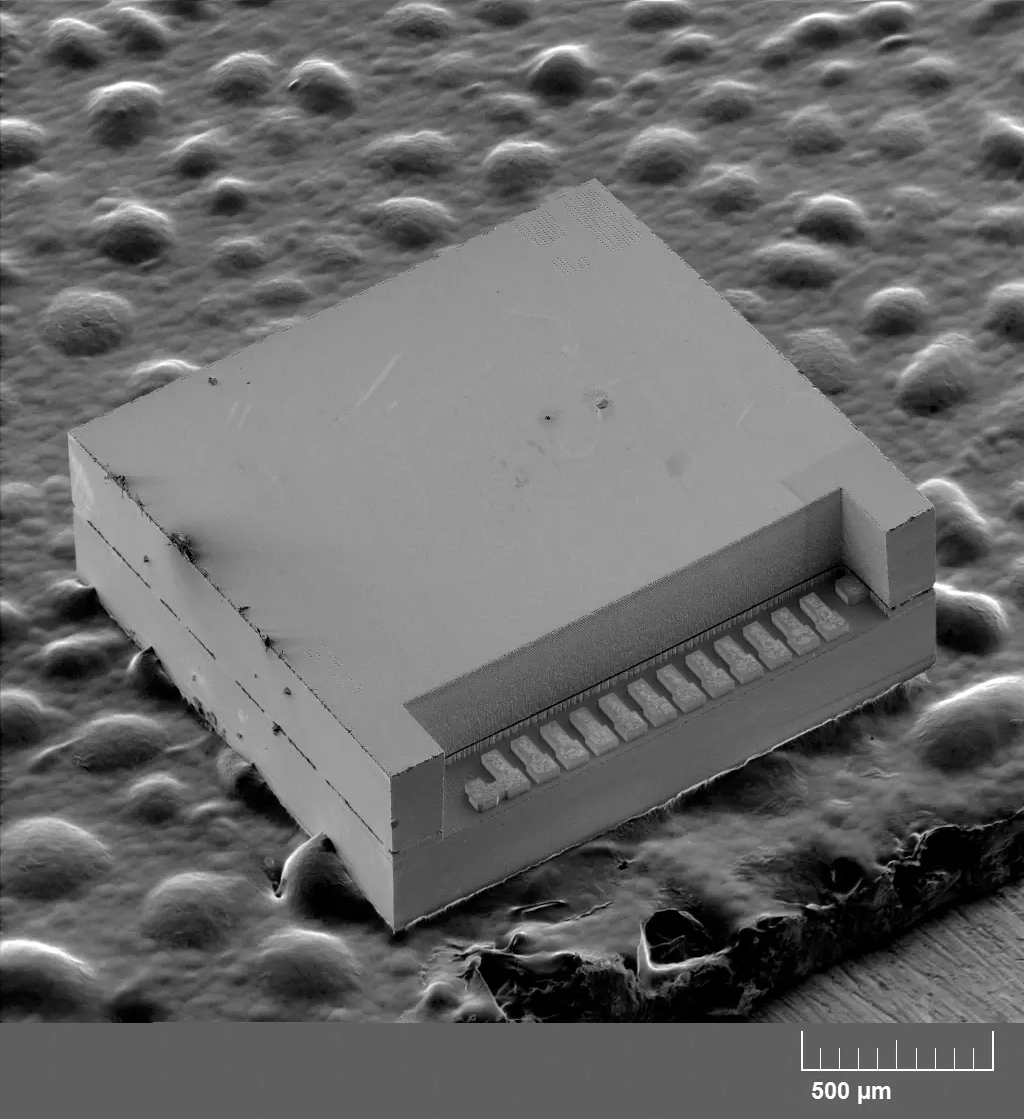
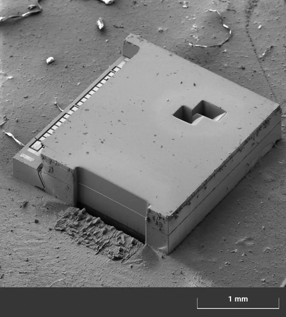
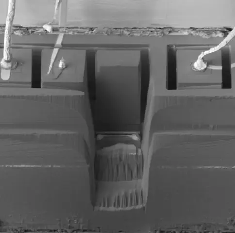
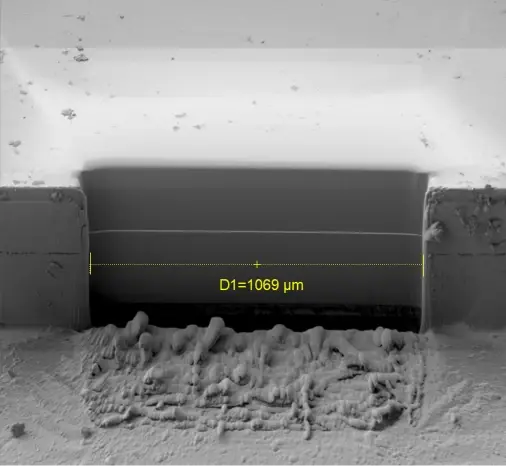
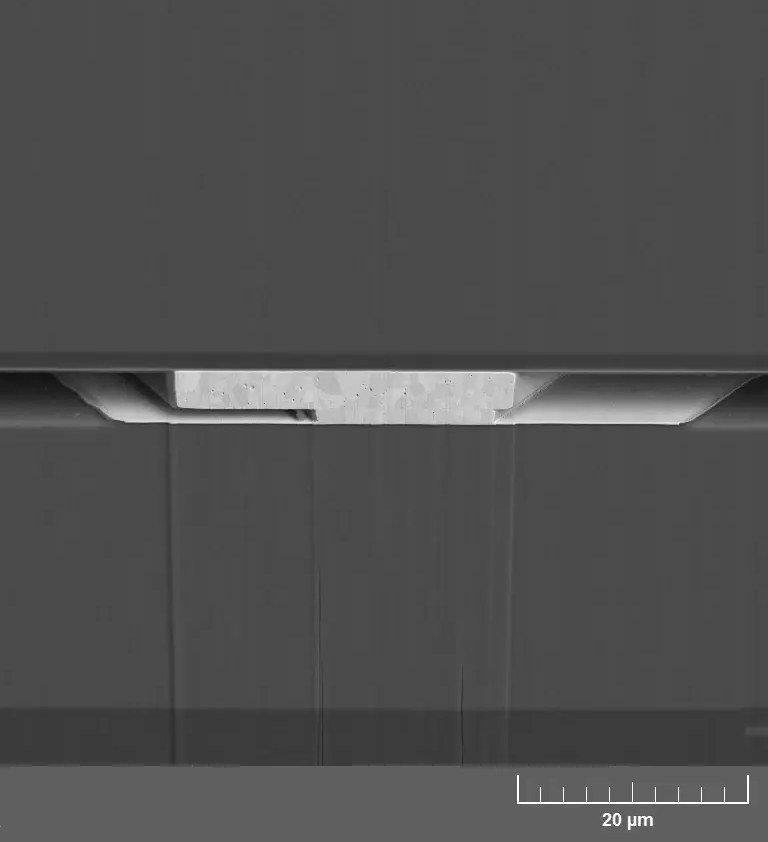
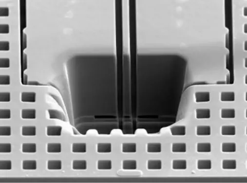
Tescan SOLARIS X™ 2 combines high-throughput Xe plasma FIB milling with advanced SEM imaging for precise, large-area cross-sectioning of MEMS devices. This integrated system enables artifact-free preparation of fragile wafer-to-wafer bonding interfaces, supporting reliable physical failure analysis of MEMS motion sensors.
You can prepare wide cross-sections, preserve delicate metallic layers, and visualize bonding seams with high contrast — all within a single, efficient workflow.
- Mistral™ Xe plasma column: delivers fast, large-area milling up to 1 mm with clean sidewalls
- Triglav™ SEM column with TriLens® optics: enables ultra-high-resolution imaging at low accelerating voltages
- Mid-Angle BSE detection: enhances contrast for metallic bonding layers and adhesion seams
- Integrated workflow control: ensures accurate endpointing and avoids delamination or structural loss
- High-throughput operation: achieve routine analysis times without compromising detail or reliability