Return to press releases
.jpg?width=352&name=Rectangle%2029183%20(1).jpg)


Do you want to reduce the time and cost of sample preparation for failure analysis?
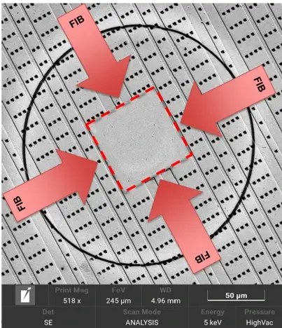
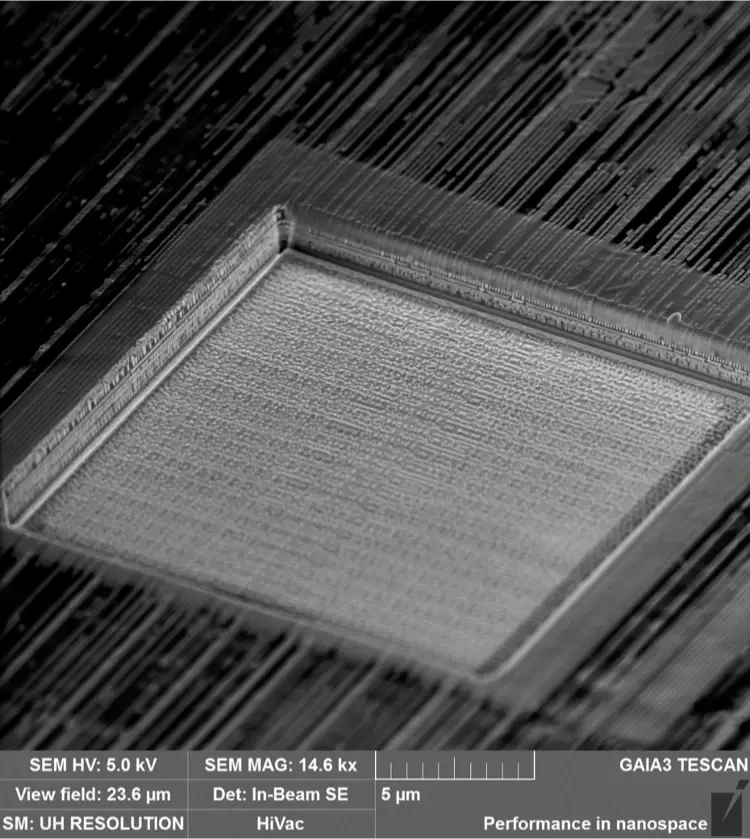
“Pairing Laser Ablation and Xe Plasma FIB-SEM: An Approach for Precise End-Pointing in Large-Scale Physical Failure Analysis in the Semiconductor Industry,” by Rodrigo Delgadillo Blando, et al., is a paper that was presented at the ISTFA conference in 2021, and it describes an innovative method for preparing large-volume cross-sections of microelectronic devices using a ps-laser ablation tool and a Xe Plasma FIB-SEM system. This is very relevant and cutting-edge research that aims to improve the efficiency and accuracy of the failure analysis of microelectronic devices.
.png)
Do you want to reduce the time and cost of sample preparation for failure analysis?
“Pairing Laser Ablation and Xe Plasma FIB-SEM: An Approach for Precise End-Pointing in Large-Scale Physical Failure Analysis in the Semiconductor Industry,” by Rodrigo Delgadillo Blando, et al., is a paper that was presented at the ISTFA conference in 2021, and it describes an innovative method for preparing large-volume cross-sections of microelectronic devices using a ps-laser ablation tool and a Xe Plasma FIB-SEM system. This is very relevant and cutting-edge research that aims to improve the efficiency and accuracy of the failure analysis of microelectronic devices.