Deliver Flat, Curtaining-Free Cross-Sections Using Tescan TRUE X-sectioning 

Combine TRUE X-sectioning with Rocking Stage to achieve curtaining-free, wide-area cross-sections for fast and reliable semiconductor failure analysis.

Increasing_FA_Throughput_in_Challenging_Samples
Unlocked content

Tescan solutions

Increase FA Throughput in Complex Packages with Tescan TRUE X-sectioning

Modern semiconductor packages such as BGAs, TSV arrays, and bond wires present major challenges for Plasma FIB workflows. Different milling rates across metals and polymers cause curtaining and terraces, while protective coatings and void filling add time without guaranteeing flat cross-sections-slowing analysis and limiting throughput.

Tescan TRUE X-sectioning with Rocking Stage solves these issues. Hard mask milling enables high-current Xe+ Plasma FIB preparation of wide, artifact-free cross-sections, while stage rocking suppresses curtaining. A ready-to-use mask library with SEM endpoint detection ensures faster, reproducible sample prep. This delivers up to 50% higher throughput for advanced failure analysis.

Why Increase Failure Analysis Throughput with Tescan TRUE X-sectioning?

Streamline Artifact-Free Cross-Sectioning with Pre-Fabricated Masks

01_Mask extracted from the pre-fabricated sample

Simplify Plasma FIB workflows with pre-manufactured hard masks that enable high-current milling without thick platinum layers. Achieve flat, curtaining-free cross-sections while reducing preparation time in complex semiconductor samples.


Enable Reliable Wide-Area Cross-Sections with Silicon Masks

02_1mm Si mask placed on the MLCC sample

Position pre-fabricated silicon masks directly onto complex samples to stabilize Plasma FIB milling. Obtain flat, artifact-free cross-sections in devices such as MLCCs without additional preparation steps.


Reveal Defects in OLED Devices with Mask-Based Cross-Sectioning

03_OLED display cross-sectioned through Si mask

Apply silicon masks to prepare clean cross-sections through fragile OLED structures. Expose delamination, layer defects, and buried interfaces with smooth, artifact-free surfaces for accurate analysis.


Expand Workflow Flexibility with a Dedicated Mask Library

04_TRUE X-Sectioning dedicated mask set_1x

Select from hundreds of pre-fabricated mask designs optimized for different FA tasks. Adapt quickly to package-level, OLED, TSV, or TEM lamella prep without complex setup or extra handling.


Improve Cross-Section Quality with Mask-Assisted Plasma FIB

05_SiC Plasma FIB cross-sectioning comparison_1x

Compare results from unmasked and masked SiC milling to see the elimination of curtaining artifacts. Achieve smooth, interpretable cross-sections that enhance accuracy in semiconductor failure analysis.


Expose Sensor Structures with Mask-Assisted Plasma FIB

06_Sensor Plasma FIB cross-sectioning through Si mask (1)

Apply silicon masks during Xe+ Plasma FIB milling to reveal clean, wide cross-sections through sensor layers. Ensure artifact-free surfaces for accurate inspection of buried interfaces and device reliability.

Contents 

01

Root of the problem

02
Materials and Methods
03
 Results and Discussion 

1. Root of the Problem

Why Conventional Plasma FIB Workflows Fall Short in Failure Analysis

Modern semiconductor packages combine metals, polymers, and void-filled structures with vastly different milling rates. Conventional Xe+ Plasma FIB workflows struggle to deliver flat cross-sections in these conditions. Terracing, ripples, and curtaining obscure fine details and reduce the accuracy of defect localization.

To compensate, analysts rely on thick platinum deposition or void filling, which add time and handling steps. Even then, large-area cross-sections remain inconsistent, and throughput drops when operators must switch to low-current milling.

Key limitations include:

  • Curtaining artifacts in heterogeneous samples
  • Extended preparation times with protective coatings
  • Extra workflow steps for void handling
  • Reduced throughput when milling at low currents

TESCAN TRUE X-sectioning with Rocking Stage overcomes these issues, enabling artifact-free, high-throughput cross-sections in today’s most complex devices.

2. Materials and Methods

How Artifact-Free Cross-Sections Were Prepared with Tescan TRUE X-sectioning

Samples included BGAs, TSV arrays, bond wires in mold compound, and OLED displays. Wide cross-sections up to 400 µm were prepared on a Tescan Xe+ Plasma FIB using hard mask-assisted TRUE X-sectioning.

Pre-fabricated silicon masks were positioned with a nanomanipulator, enabling high-current milling without thick platinum layers or void filling. The Rocking Stage tilted samples during milling, reducing curtaining and topography-driven artifacts.

Live SEM imaging provided endpoint detection for precise defect targeting. The same workflow was also applied to TEM lamellae, demonstrating versatility across failure analysis tasks.

This approach delivered large-area, artifact-free cross-sections at high currents—cutting preparation time and improving reproducibility in complex devices.

3. Results and Discussion

TRUE X-sectioning Delivers Flat, High-Throughput Cross-Sections in Complex Devices

Tescan TRUE X-sectioning with Rocking Stage enabled wide, artifact-free cross-sections in BGAs, TSV arrays, OLED displays, and sensor packages. High-current Xe+ Plasma FIB milling with hard masks eliminated curtaining and terraces, producing smooth, interpretable surfaces for defect localization.

SEM endpoint detection ensured precise targeting of buried structures, while the same workflow supported reproducible TEM lamella preparation. Compared to conventional workflows, TRUE X-sectioning reduced preparation time by up to 50% without compromising quality.

These results demonstrate that mask-assisted Plasma FIB and Rocking Stage technology combine throughput and surface integrity—providing reliable, consistent failure analysis across the most challenging semiconductor samples.

Unlock 
tescan insight

leave a contact to access

Get the most out of Tescan

This is more than information; it's an advantage. We've compiled our technical whitepapers, detailed product flyers, and on-demand webinars to provide you with the knowledge that makes a real difference. Sign up now to access the insights you need to make an impact.

Tescan Instruments & Technology

Used in This Workflow

Tescan Plasma FIB-SEM – High-Throughput Xe+ Ion Milling
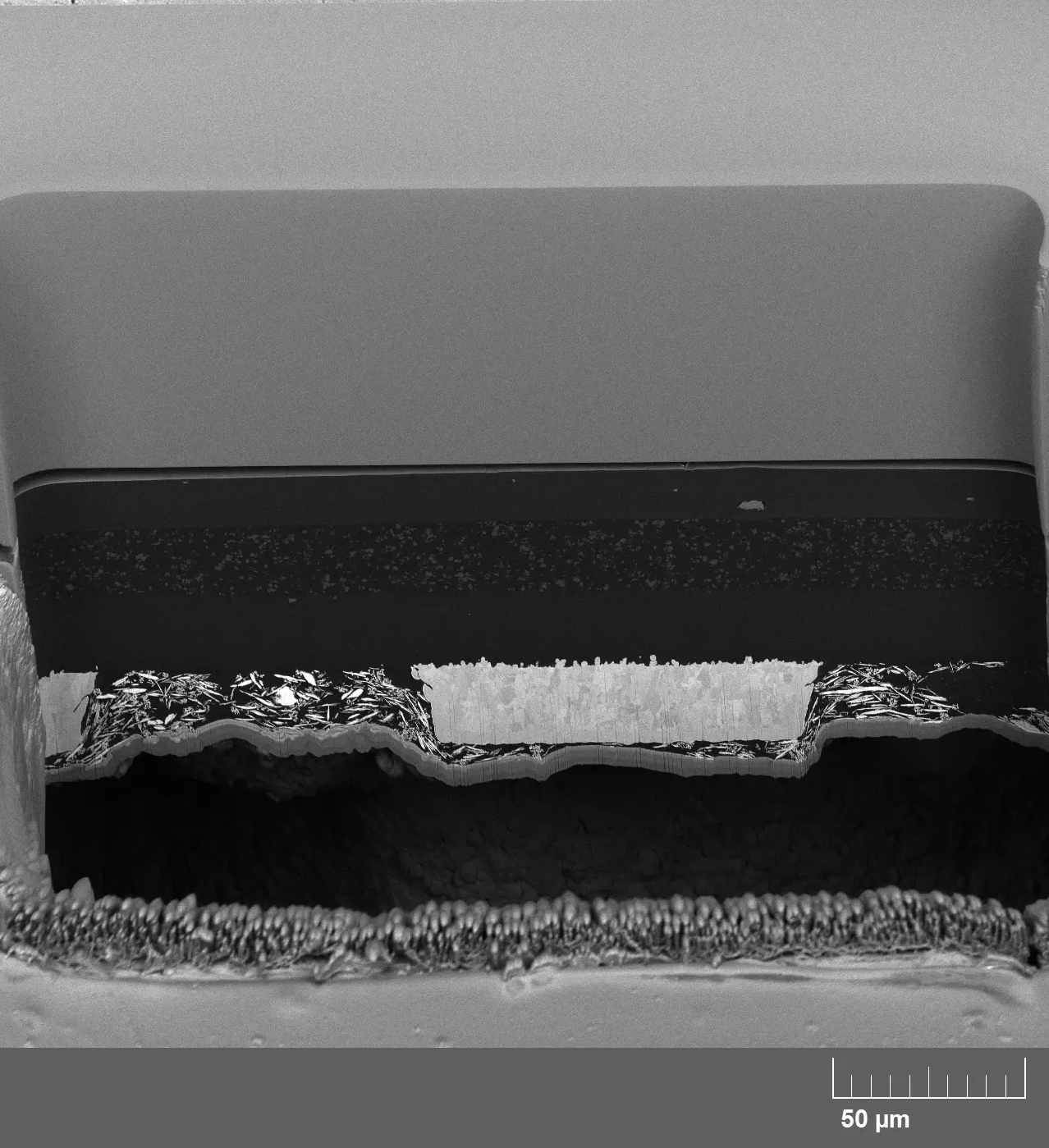
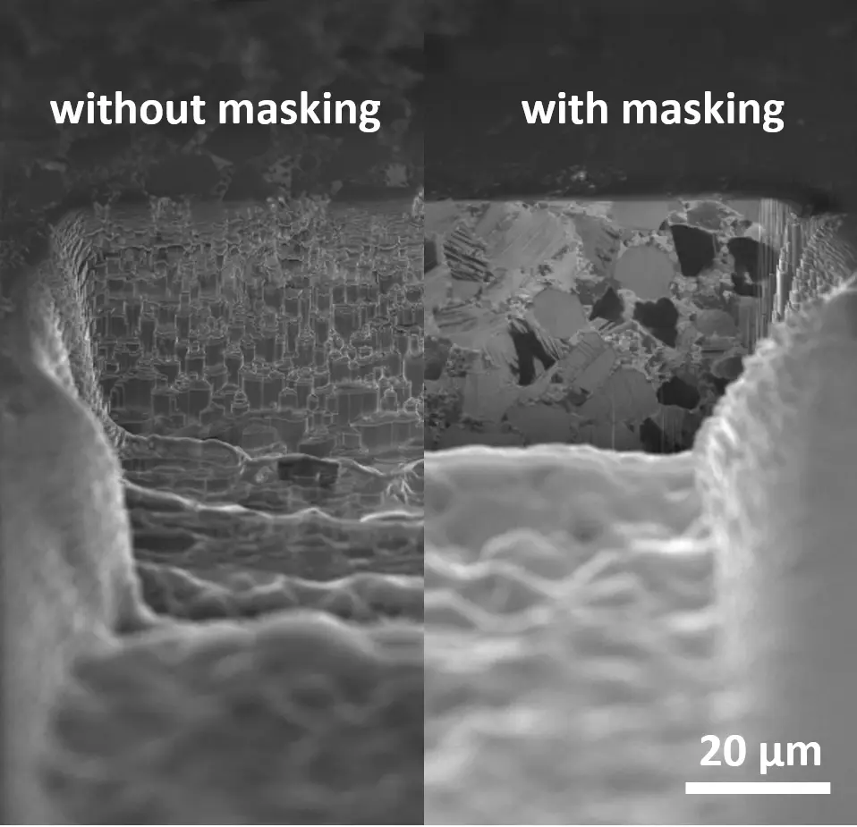
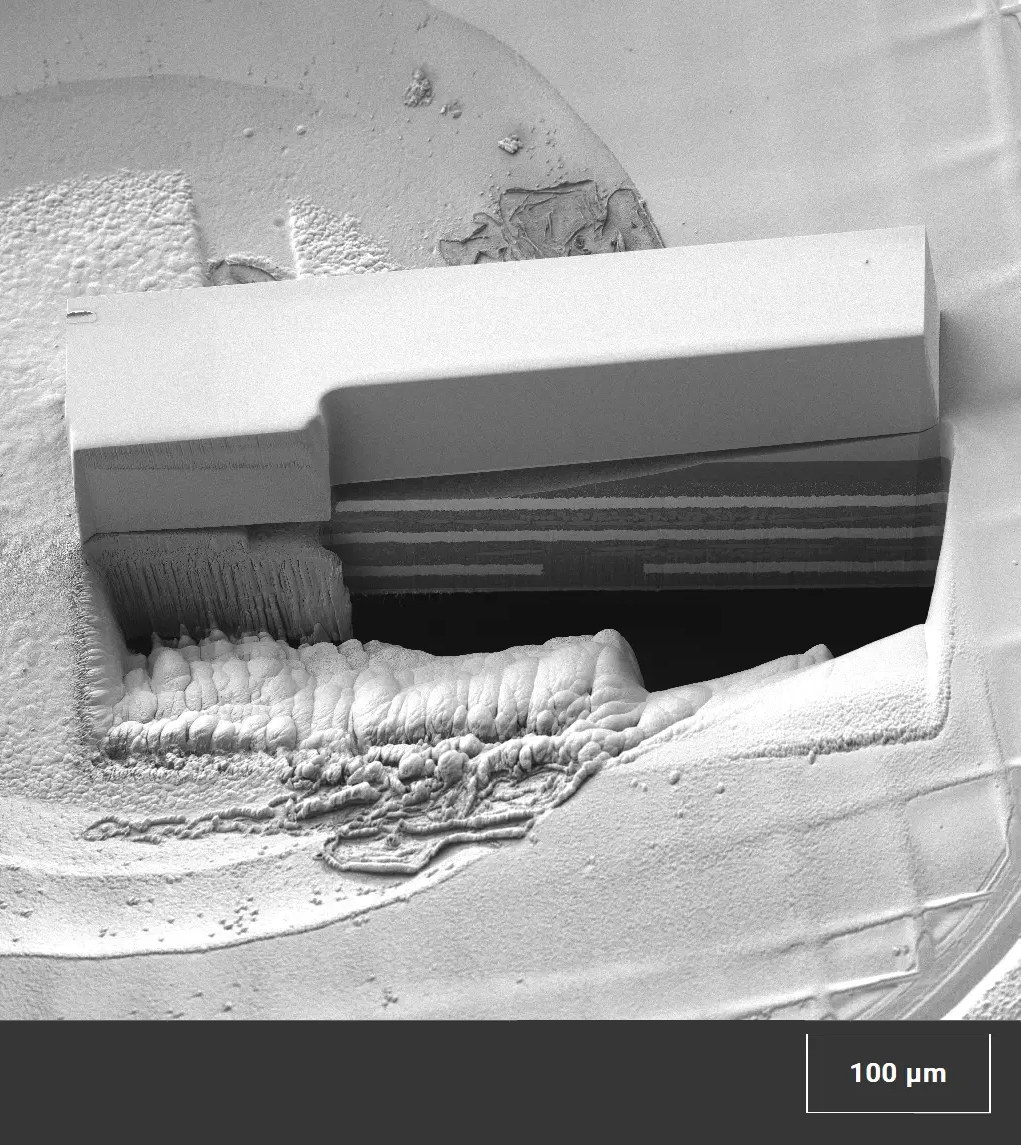
TESCAN Plasma FIB-SEM systems use Xe+ ions for high-current milling and wide-area cross-sections. They integrate SEM imaging and Plasma FIB precision, enabling preparation of cross-sections hundreds of micrometers wide.


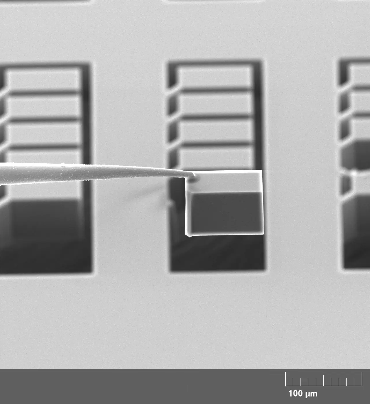
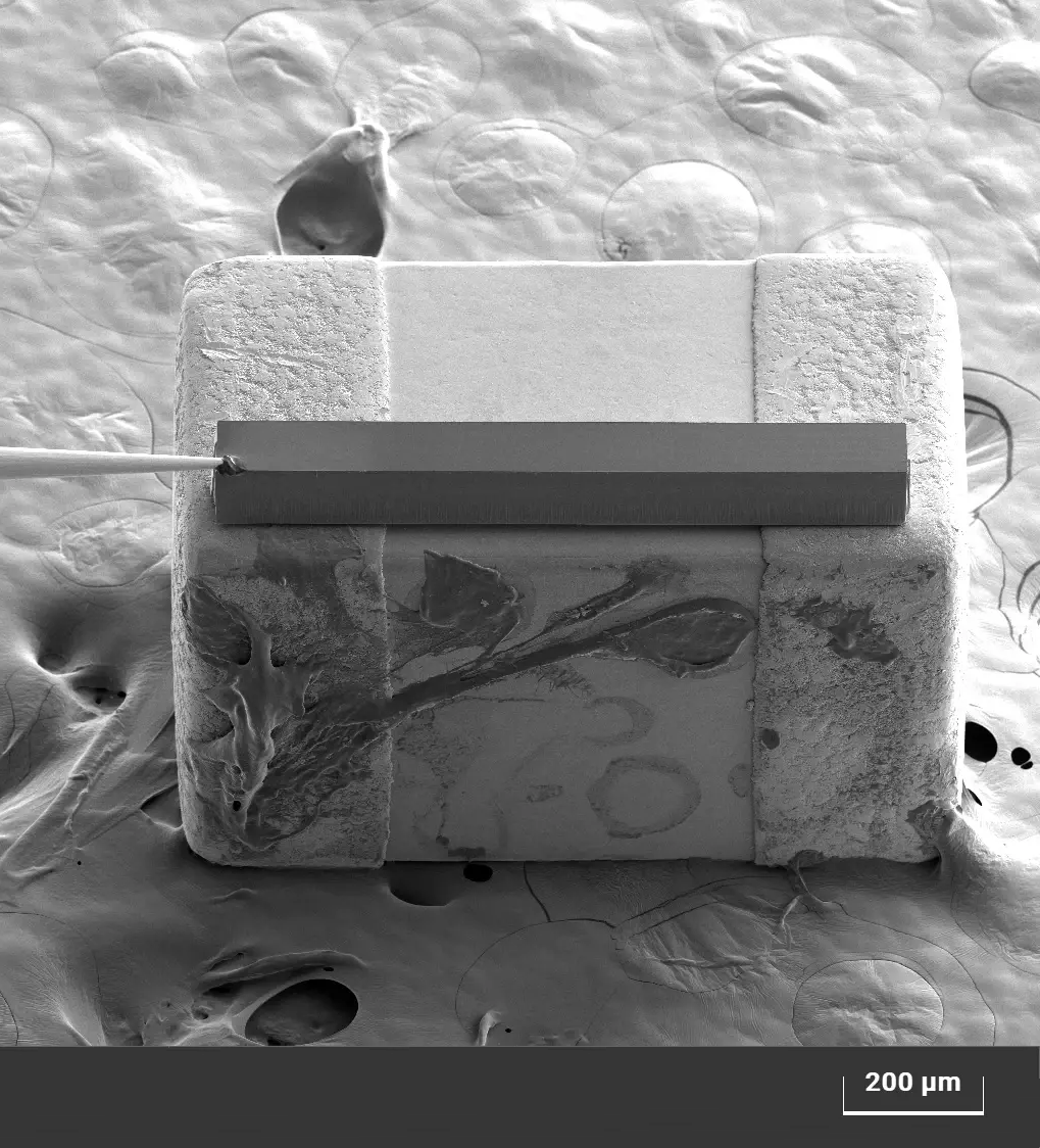
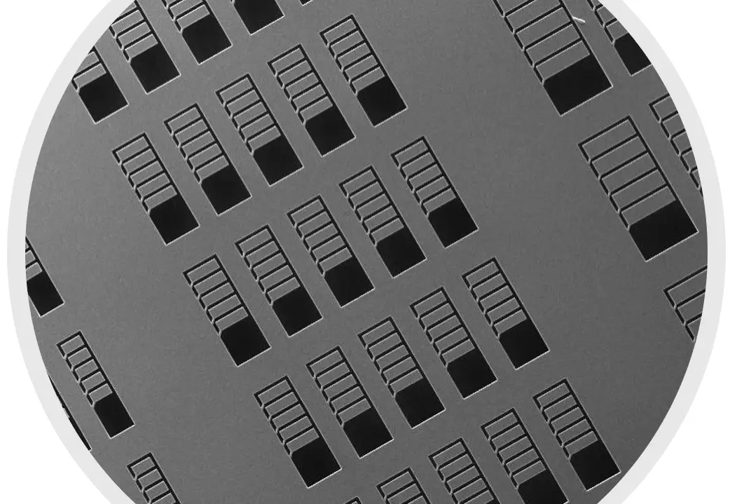
Analyze BGAs, TSVs, bond wires, OLEDs, and sensors with artifact-free surfaces, prepare TEM lamellae, and use live SEM endpoint detection for accurate targeting—all in one workflow.

  • Xe+ Plasma FIB: high-current milling for wide cross-sections

  • Integrated SEM: real-time endpoint detection

  • Large-area prep: up to 400 µm without artifacts

  • Ga-free source: minimizes amorphization

  • Multi-application use: FA, OLEDs, TSVs, lamella prep 

Tescan Rocking Stage – Curtaining Suppression

The Rocking Stage tilts samples during Plasma FIB milling to suppress curtaining in multi-material structures. It delivers smooth surfaces across wide areas while supporting high-current milling speeds.

  • Active sample rocking: reduces curtaining and terraces

  • Wide-area compatible: preserves surface integrity

  • Streamlined prep: less need for coatings or void filling

  • High-throughput: artifact-free at high beam currents

Tescan TRUE X-sectioning Mask Set – Pre-Fabricated Hard Masks

The TRUE X-sectioning mask set contains hundreds of pre-fabricated hard masks for artifact-free Plasma FIB cross-sectioning. Masks are placed with a nanomanipulator, enabling high-current milling without thick platinum layers or void filling.


Select from a versatile library for BGAs, TSVs, OLEDs, sensors, and TEM lamella workflows with faster turnaround and reproducible quality.

  • Pre-fabricated masks: ready for immediate use

  • Hard mask milling: flat, curtaining-free surfaces

  • Versatile library: 970 designs for diverse tasks

  • Efficiency boost: reduces prep time by up to 50%

  • SEM endpoint detection: precise defect targeting 

GET IN Touch

Contact us

map

Where can you find us:

Tescan Brno
Libušina třída 21
623 00 Brno 
Czech Republic

info@Tescan.com