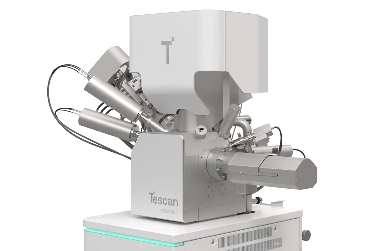
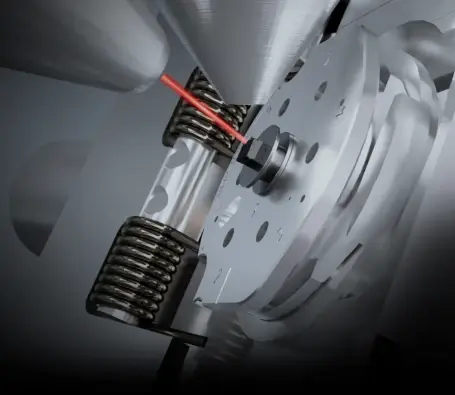
Tescan SOLARIS X™ 2 with Rocking Stage™
Tescan SOLARIS X™ 2 with Rocking Stage™ combines high-throughput Xe plasma FIB milling with simultaneous SEM observation to deliver smooth, artifact-free cross sections in complex semiconductor structures.
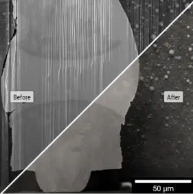
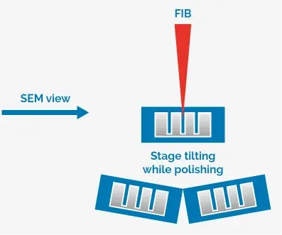
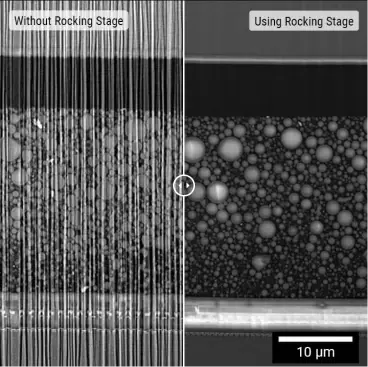
The integrated Rocking Stage™ introduces tilt in the plane of the cross section, reducing curtaining and enabling precise endpointing during polishing.
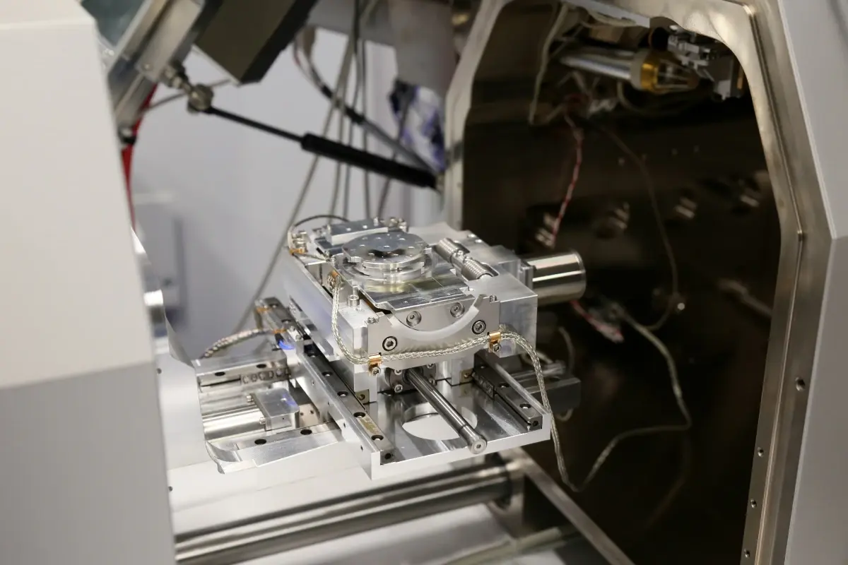
- Rocking Stage™ integration: enables alternating-angle milling for smoother surfaces
- Continuous SEM/BSE observation: supports real-time monitoring and accurate endpoint detection
- Xe plasma FIB technology: provides fast material removal for large-area cross sections
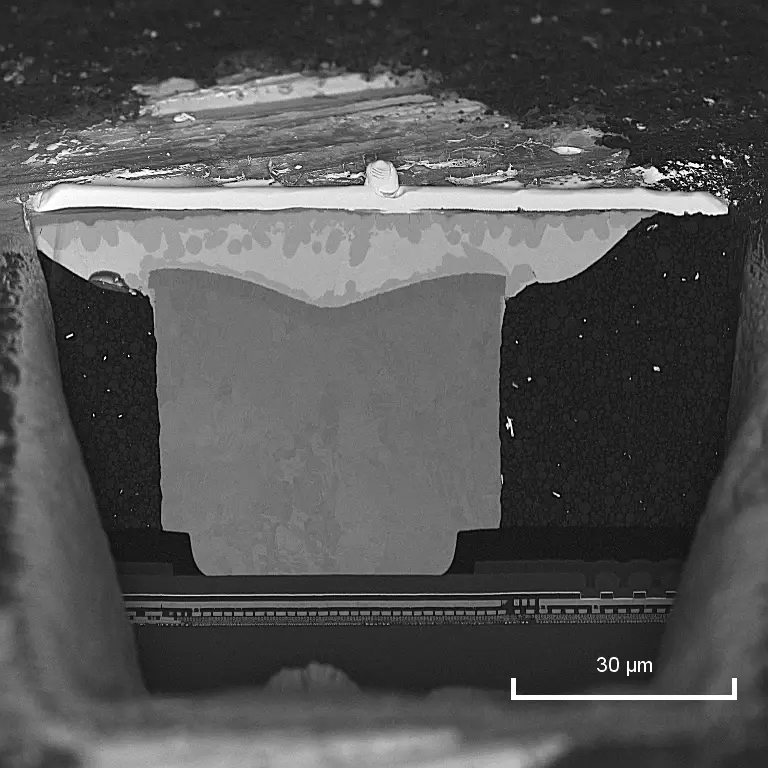
- Improved surface integrity: preserves interfaces in solder bumps, TSVs, and copper pillars
- Streamlined workflow: eliminates repositioning steps and reduces preparation time