Tescan SOLARIS X™ 2 Plasma FIB-SEM
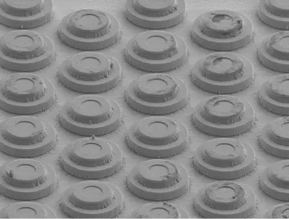
Tescan SOLARIS X™ 2 gives you the precision, beam current, and stability needed for large-area cross-sectioning of OLED and Micro-LED displays.
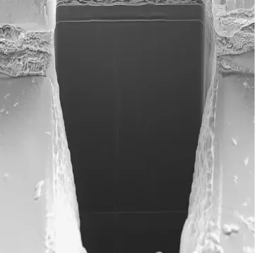
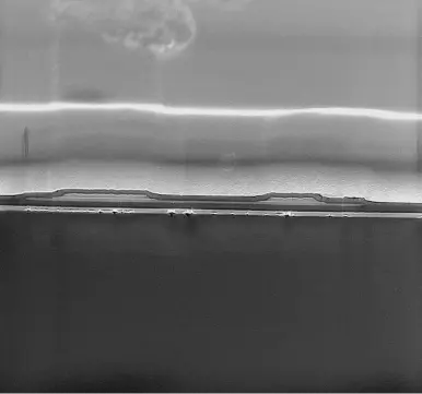
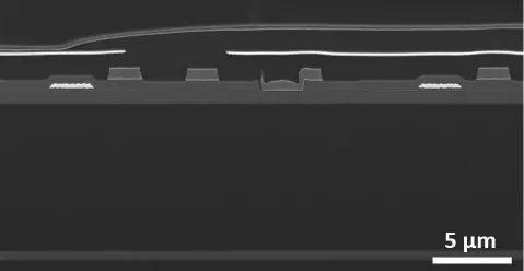
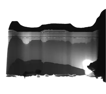
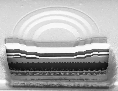
With a high-current Xe plasma FIB and integrated SEM, you can mill uniform trenches up to 1 mm wide—without causing delamination or layer distortion. Optimized detectors provide clear imaging of polyimide, ITO, and other thin-film materials, even in beam-sensitive regions.
From alignment to final inspection, SOLARIS X™ 2 supports a seamless workflow for high-contrast, artifact-free cross-sections.
- High-current Xe plasma FIB: Fast, precise milling across wide display regions
- Integrated SEM and FIB system: Complete prep and imaging in one tool
- Low-kV SEM imaging: Protects sensitive OLED materials during inspection
- Mid-angle BSE and SE detectors: Improve contrast in complex layer stacks
- Stable cross-sectioning: Preserves interface clarity across hundreds of microns