Tescan SOLARIS X™ 2 with Xe Plasma FIB-SEM
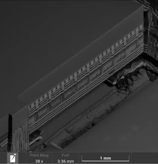
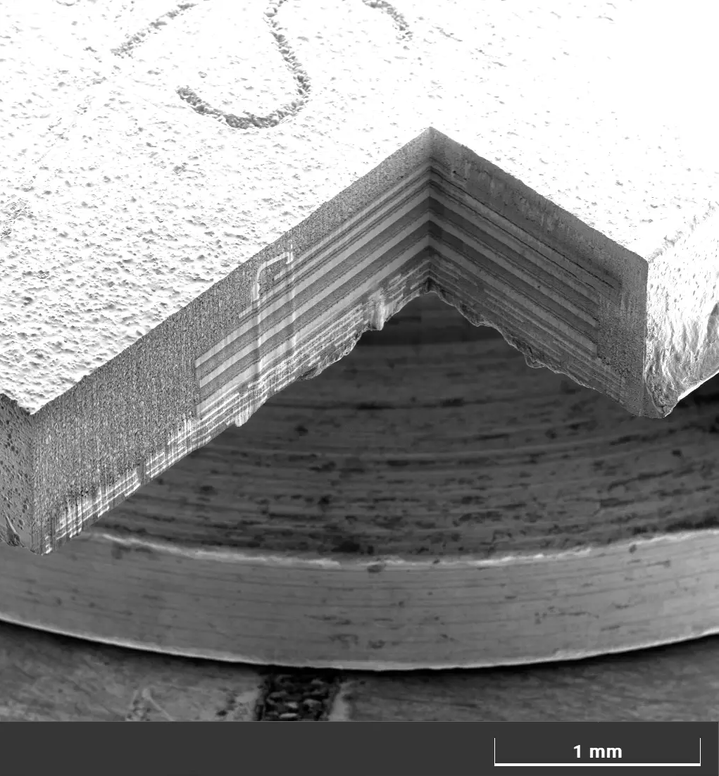
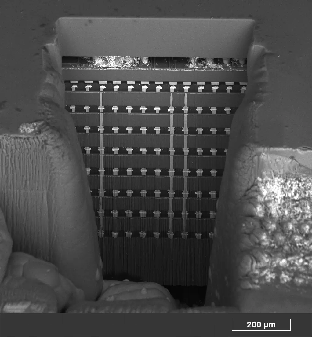
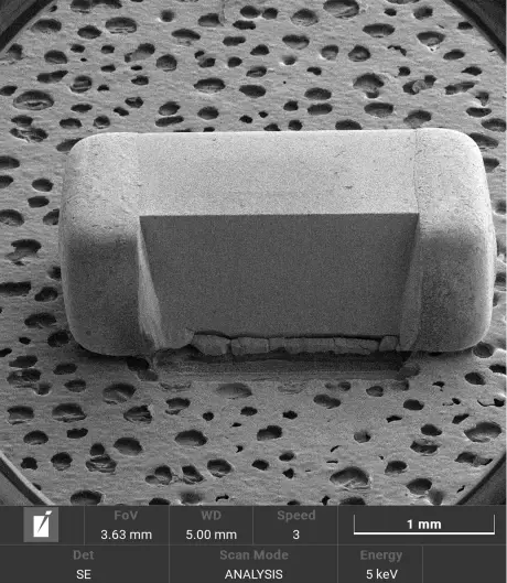
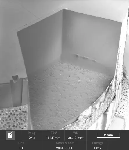
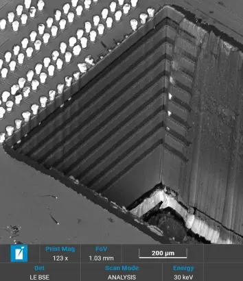
Tescan SOLARIS X™ 2 combines high-throughput Xe plasma FIB milling with high-resolution SEM imaging to prepare large, geometry-true cross-sections of complex semiconductor devices. Its wide current range and precision control make it ideal for both rapid bulk removal and fine surface polishing.
- Xe plasma FIB: enables fast removal of millimeter-scale volumes without thermal damage
- SEM column: delivers high-resolution imaging for surface inspection and analysis
- Large-current range (up to 3.3 μA): supports both speed and precision in a single system
- True X-Sectioning: ensures clean, artifact-free surfaces ready for SEM/EDS analysis
- Automation-ready platform: reproducible workflows for semiconductor failure analysis