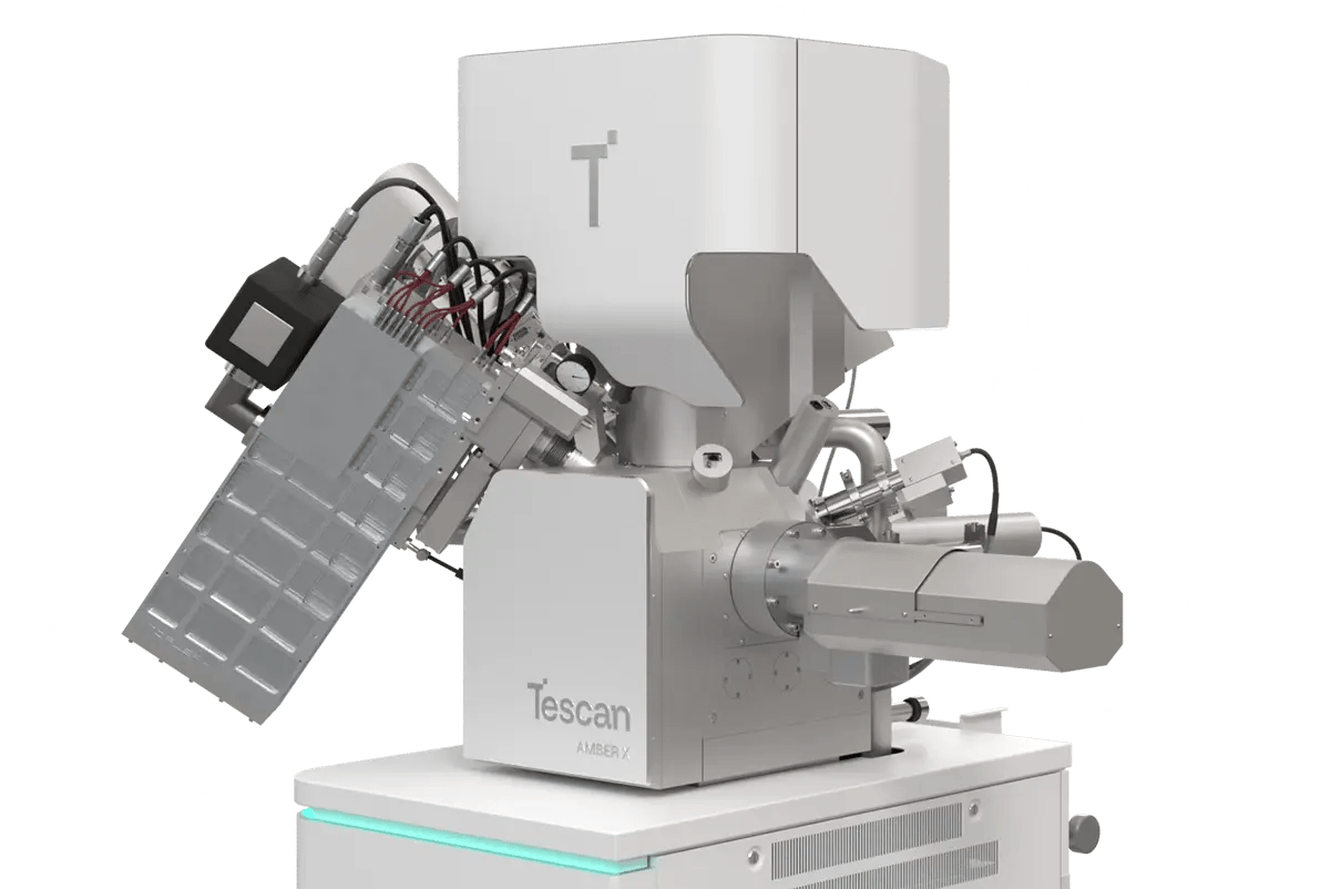
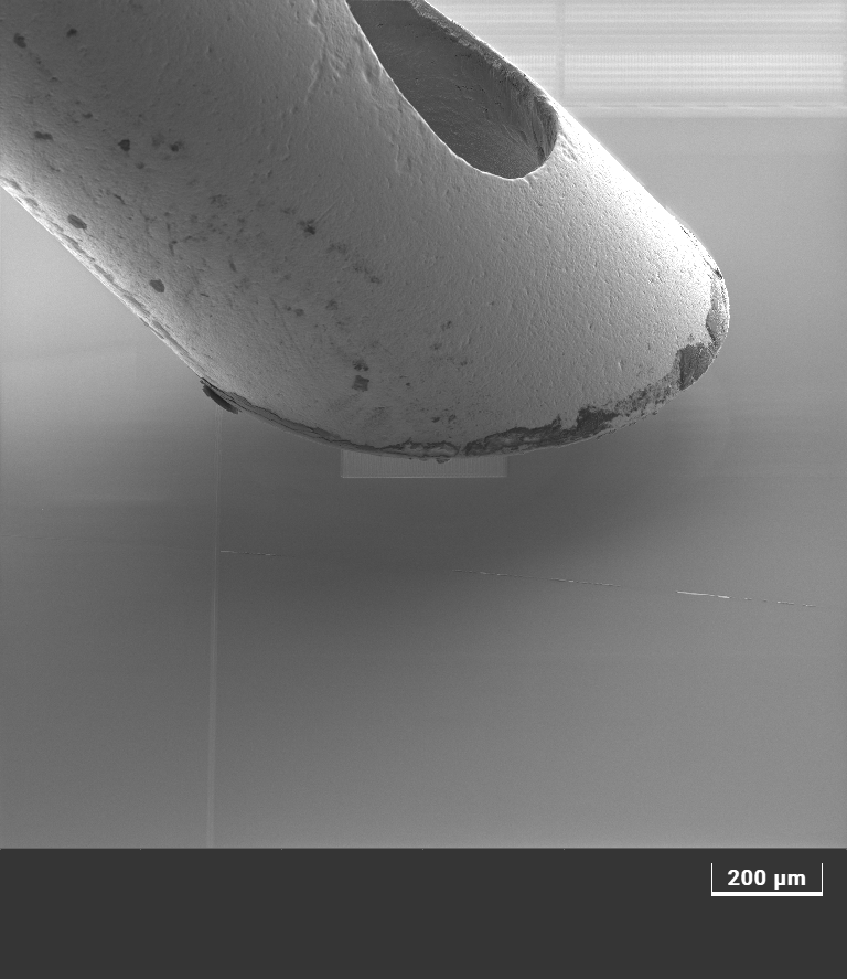
Tescan AMBER X™ 2 Plasma FIB-SEM
Tescan AMBER X™ 2 Plasma FIB-SEM combines a high-throughput Xe+ plasma FIB with a field-free UHR SEM column, enabling large-area delayering and ultra-high-resolution imaging in a single workflow.
Designed for advanced semiconductor failure analysis, it delivers precise control, uniform planarity, and direct integration with in-situ nanoprobing.
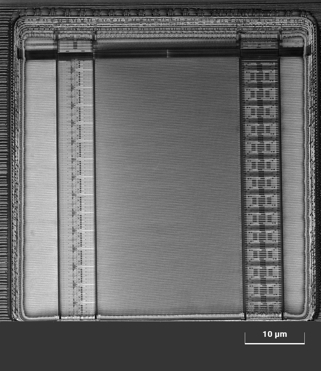
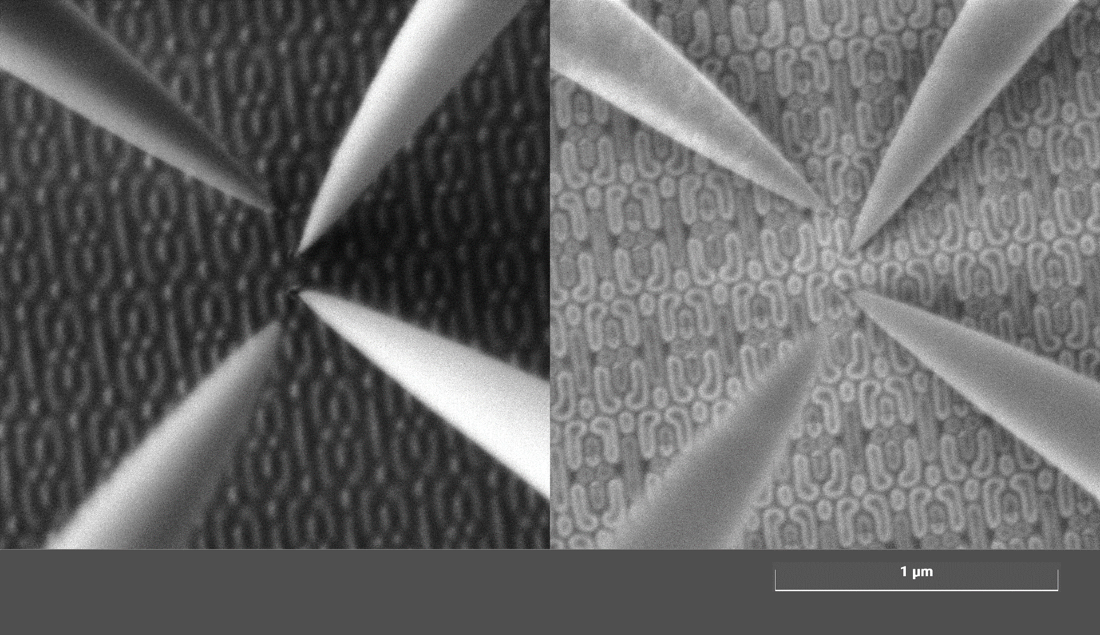
You can delayer complex logic and memory devices, expose transistor layers with real-time endpoint detection, and prepare contamination-free surfaces optimized for electrical probing and TEM readiness.
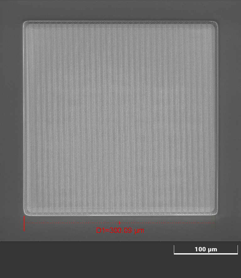
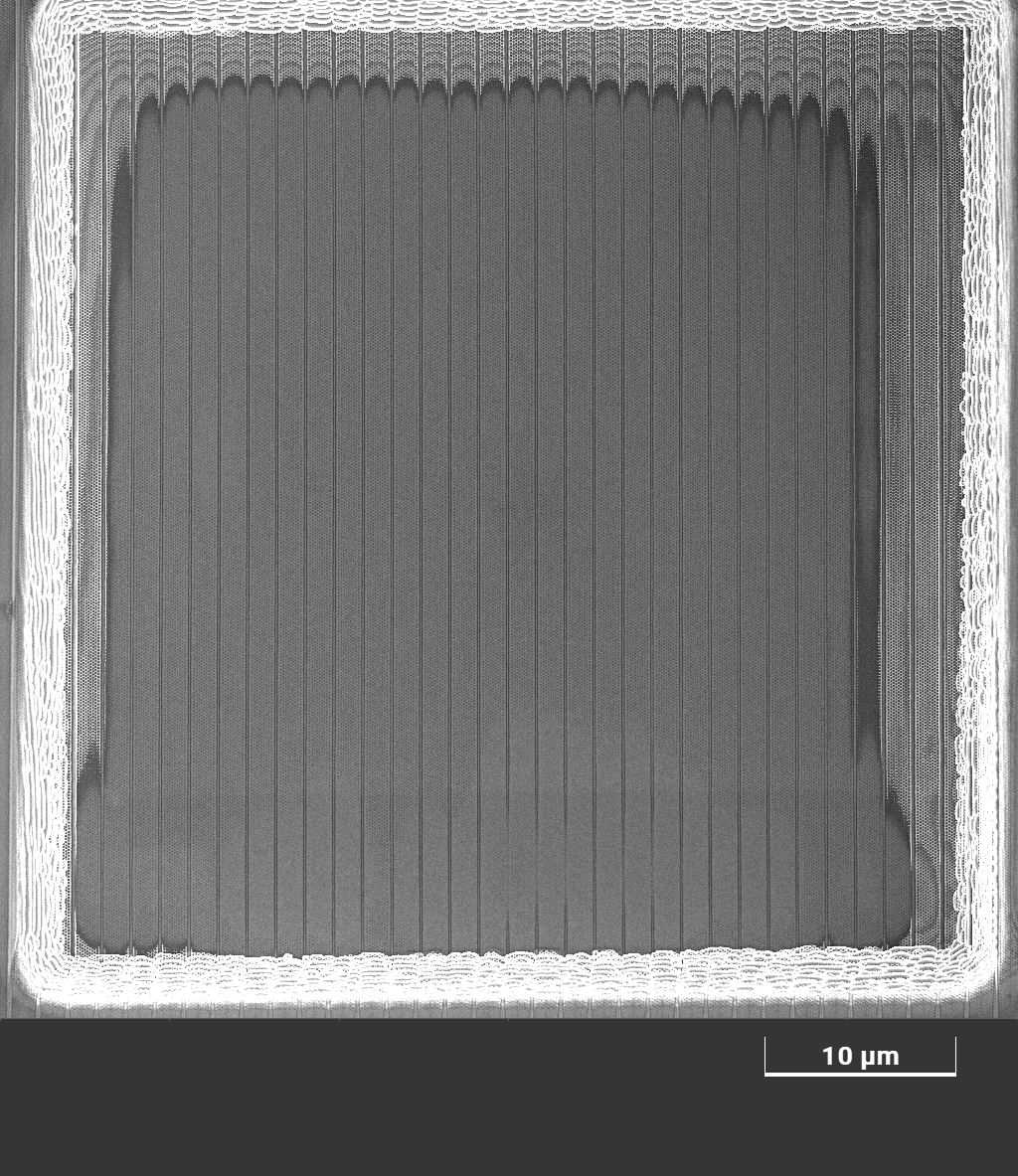
- Xe+ plasma FIB: high-throughput milling for large-area delayering of sub-20 nm nodes
- Field-free UHR SEM: ultra-high-resolution imaging without magnetic interference
- Mistral™ Plasma FIB: low keV gentle layer removal during delayering
- Real-time SE signal end pointing: accurate transistor exposure without over-milling
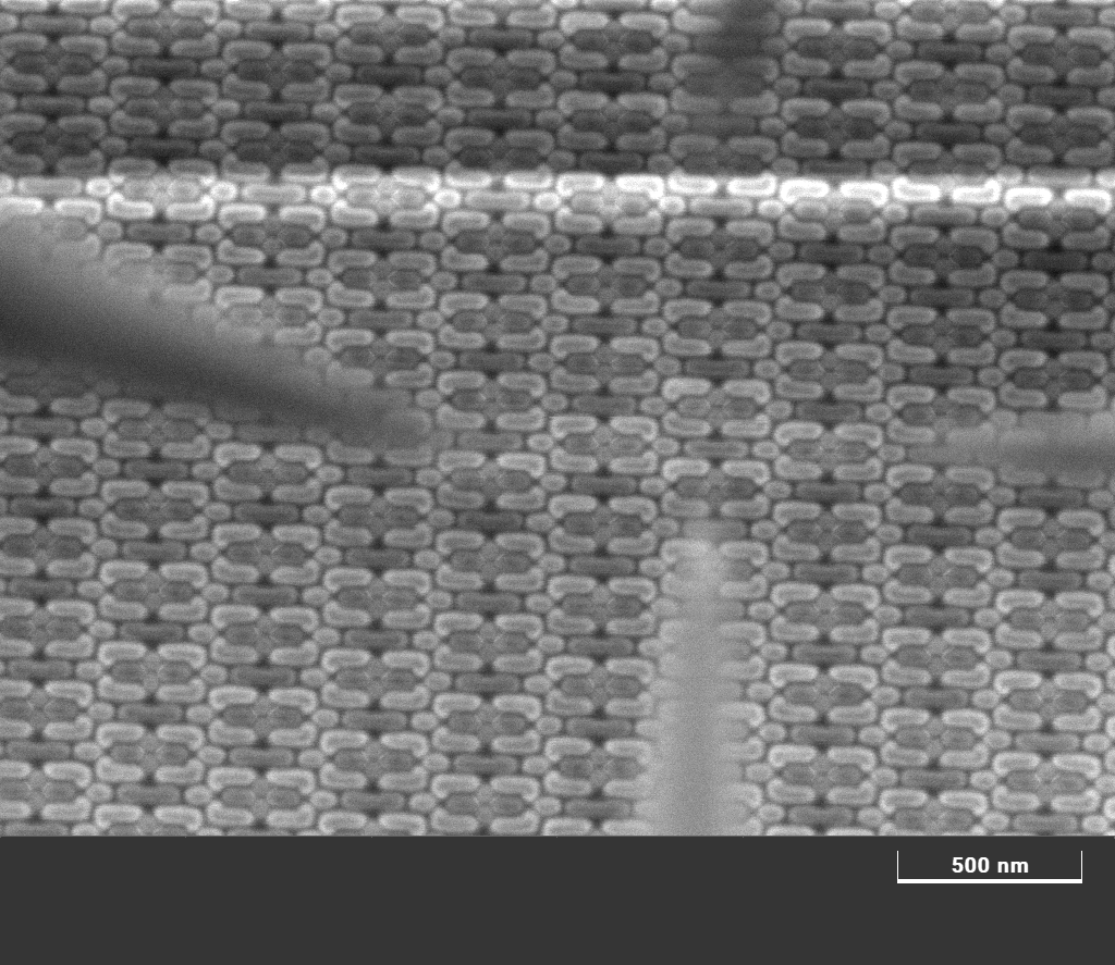
- Nanoflat etch: dielectric surface smoothing below 5 nm RMS roughness
- Nanoflat gas chemistry: selective copper removal with oxidation-free surfaces
- In-situ nanoprobing compatibility: seamless integration with Kleindiek PS8 for electrical analysis