The semiconductor industry’s relentless race for high integration, high density, and miniaturization of microelectronic devices has resulted in the development of new technologies such as 3D ICs that make it possible to integrate extensive functionality into ever smaller, faster, and lower power consumption devices. TESCAN SOLARIS X pairs the high-throughput i-FIB+™ Xe plasma FIB column with the Triglav™ UHR electron column to extend the capabilities of FIB physical failure analysis to include large-area and deep cross-sectioning on advanced packaging, microelectromechanical devices, and optoelectronics. Please join our webinar on TESCAN SOLARIS X for Semiconductors. Besides deep sectioning, the webinar will examine the wider potential of SOLARIS X for a Ga-free TEM sample preparation and homogenous FIB delayering of sub-14 nm technology nodes.
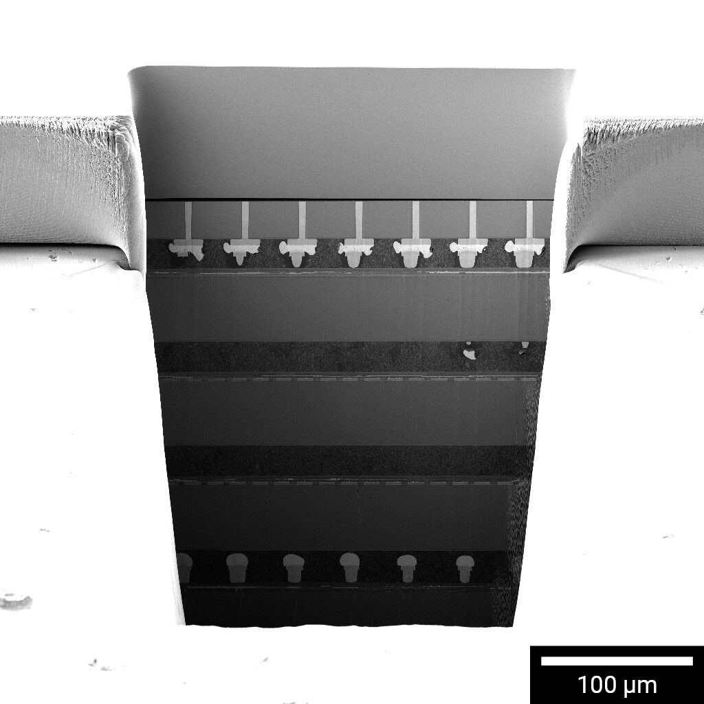
Large scale Plasma FIB cross-section of 2.5D IC through center of both TSV and microbump array, 2 kV SE image.
Presenter: Lukas Hladik
About Lukas Hladik
Lukas Hladik is a Product Manager for FIB-SEM, characterization, and delayering/probing solutions for FA semiconductor R&D labs. He joined TESCAN ORSAY HOLDING in 2012 as an application specialist for Plasma FIB-SEM platforms. All his work in TOH has been connected extensively with the worldwide semiconductor industry. Lukas has a Master’s degree in Physical Engineering and Nanotechnology from Brno University of Technology, Brno, Czech Republic.