Prepare Top-down, Inverted and Planar TEM lamella from Logic and Memory Devices
On demand
ENGLISH
The global integrated circuit (IC) industry is facing higher demand for electronic devices that offer improvements in device performance and energy consumption—as well as decreased device footprint. In order to achieve this, TEM lamella preparation has become an inevitable part of the failure analysis process.
The 3D structure of today’s devices requires the localization of defects in different projections. The shrinking device size dictates the need to use inverted TEM lamella geometry to achieve sub-10 nm lamella thickness. With defect size now at the nm-scale, there is an additional need for plan-view TEM lamella geometry for STEM observation. Thus, TEM lamella lift-out procedures might require multiple manipulation steps or even breaking the vacuum to reach inverted or plan-view lamella geometries. TESCAN SOLARIS addresses these challenges with a patented setup that enables lamella transfer from a bulk sample onto a TEM grid with a single, simple manipulation step, and no need to break the vacuum or unload the sample. Most importantly, this approach does not require any additional hardware to be installed.
This webinar will provide insight into how TESCAN SOLARIS and its ecosystem can be utilized for semi-automated, high-quality, low beam damage sample preparation in the semiconductor FA lab environment.
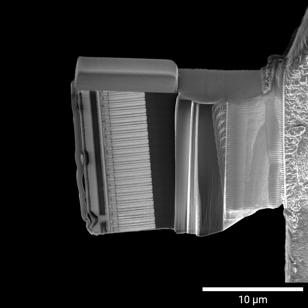
TEM lamella from a 3D-NAND memory device in a 100° vertical geometry to avoid curtaining artifacts, 2 kV In-Beam SE image.
Presenter: Lukas Hladik
About Lukas Hladik
Lukas Hladik is a Product Manager for FIB-SEM, characterization, and delayering/probing solutions for FA semiconductor R&D labs. He joined TESCAN ORSAY HOLDING in 2012 as an application specialist for Plasma FIB-SEM platforms. All his work in TOH has been connected extensively with the worldwide semiconductor industry. Lukas has a Master’s degree in Physical Engineering and Nanotechnology from Brno University of Technology, Brno, Czech Republic.